IC substrate having over voltage protection function

a technology of over voltage protection and substrate, applied in the direction of overvoltage protection resistors, thin film varistors, basic electric elements, etc., can solve the problems of high design cost, limited space, and inability to recover damage to the ic devi

Inactive Publication Date: 2006-05-30
INPAQ TECH
View PDF32 Cites 34 Cited by
  • Summary
  • Abstract
  • Description
  • Claims
  • Application Information

AI Technical Summary

Benefits of technology

[0006]An object of the present invention is to provide an IC substrate with over voltage protection functions and a method for manufacturing the same and thus, the IC device can be protected against the presence of surge pulses.

Problems solved by technology

Because such structure cannot provide over voltage protection functions, the IC device cannot withstand the energy of surge pulses, which result in an irrecoverable damage to the IC device.
Therefore, such design has the disadvantages of high design costs, wasting limited space, and providing incomplete protection for the IC device.

Method used


Image

  • IC substrate having over voltage protection function
  • IC substrate having over voltage protection function
  • IC substrate having over voltage protection function

Examples


Embodiment Construction

[0025]The embodiments of the present invention are described with reference to the drawings. The same elements in the drawings have the same reference numerals.

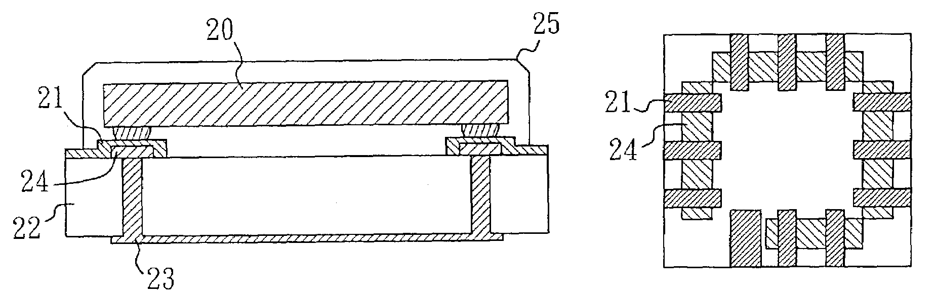
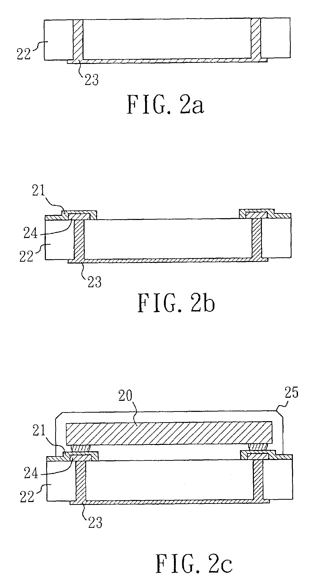
[0026]FIGS. 2a, 2b and 2c are sectional views of an IC substrate formed with over voltage protection functions according to an embodiment of the present invention. As shown in FIG. 2a, a first conductor layer is formed to be a grounding conductor layer (23) on a substrate (22). The first conductor layer is formed on a lower surface of the substrate and extends through the substrate to its upper surface. One or more terminals are formed on the upper surface of the substrate. As shown in FIG. 2b, one or more variable resistance material layers (24) are formed to overlay the terminals of the grounding conductor layer (23) so as to form connection with each of the variable resistance material layers. In addition, a plurality of second conductor layers (21) are formed to be upper electrodes. The second conductor layers overlay on ...


PUM


Abstract

The present invention relates to an IC substrate provided with over voltage protection functions and thus, a plurality of over voltage protection devices are provided on a single substrate to protect an IC chip directly. According to the present invention, there is no need to install protection devices at respective I/O ports on a printed circuit board to prevent the IC devices from damage by surge pulses. Therefore, the costs to design circuits are reduced, the limited space is efficiently utilized, and unit costs to install respective protection devices are lowered down.

Description

FIELD OF THE INVENTION[0001]The present invention relates to an IC substrate with over voltage protection functions, more particularly, to an IC substrate provided with a structure having multiple over voltage protection devices.BACKGROUND OF THE INVENTION[0002]A conventional over voltage protection device is installed near I / O ports on a printed circuit board to protect internal IC devices according to demands by each IC device. However, such design requires installing independent over voltage protection devices in accordance with requirements of respective circuits to prevent respective IC devices from being damaged by surge pulses.[0003]Please refer to FIG. 1a, which is a top view of an IC device disposed on a conventional substrate. In FIG. 1a, there are a plurality of electrodes (11) and a grounding line (13) disposed on a substrate (12). Then, an IC device (10) is soldered to the plurality of electrodes and the grounding line. FIG. 1b is a sectional view of the IC device dispo...

Claims


Application Information

Patent Timeline
Patent Type & Authority Patents(United States)
IPC IPC(8): H01L23/48H01C7/04H01L23/52H01L23/12H01C7/10H01C7/12H01L21/48H01L23/62
CPCH01C7/1013H01L21/4857H01L21/486H01L23/057H01L23/49816H01L23/49822H01L23/49827H01L23/50H01L23/62H01L24/48H01C7/12H01L2224/16235H01L24/10H01L2224/05599H01L2224/16H01L2224/48091H01L2224/48247H01L2224/4826H01L2224/48472H01L2224/85399H01L2924/01079H01L2924/014H01L2924/14H01L2924/15311H01L2924/19105H01L2924/19106H01L2224/0401H01L2924/01033H01L2924/01006H01L2924/01005H01L2924/00014H01L2224/45099H01L2924/00H01L2924/15787H01L2924/12042H01L23/12
Inventor LEE, CHUN-YUAN
Owner INPAQ TECH
Why Eureka
Try Eureka