Laser repair structure of liquid crystal display device and method thereof
a liquid crystal display and laser repair technology, applied in non-linear optics, instruments, optics, etc., can solve the problems of unusable crt, unexpected particles deposited in tft under manufacturing procedures, and occupy a lot of conventional cathode-ray tubes (crts) , to achieve the effect of increasing conductivity
- Summary
- Abstract
- Description
- Claims
- Application Information
AI Technical Summary
Benefits of technology
Problems solved by technology
Method used
Image
Examples
first embodiment
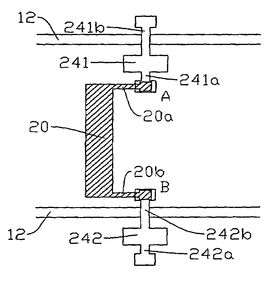
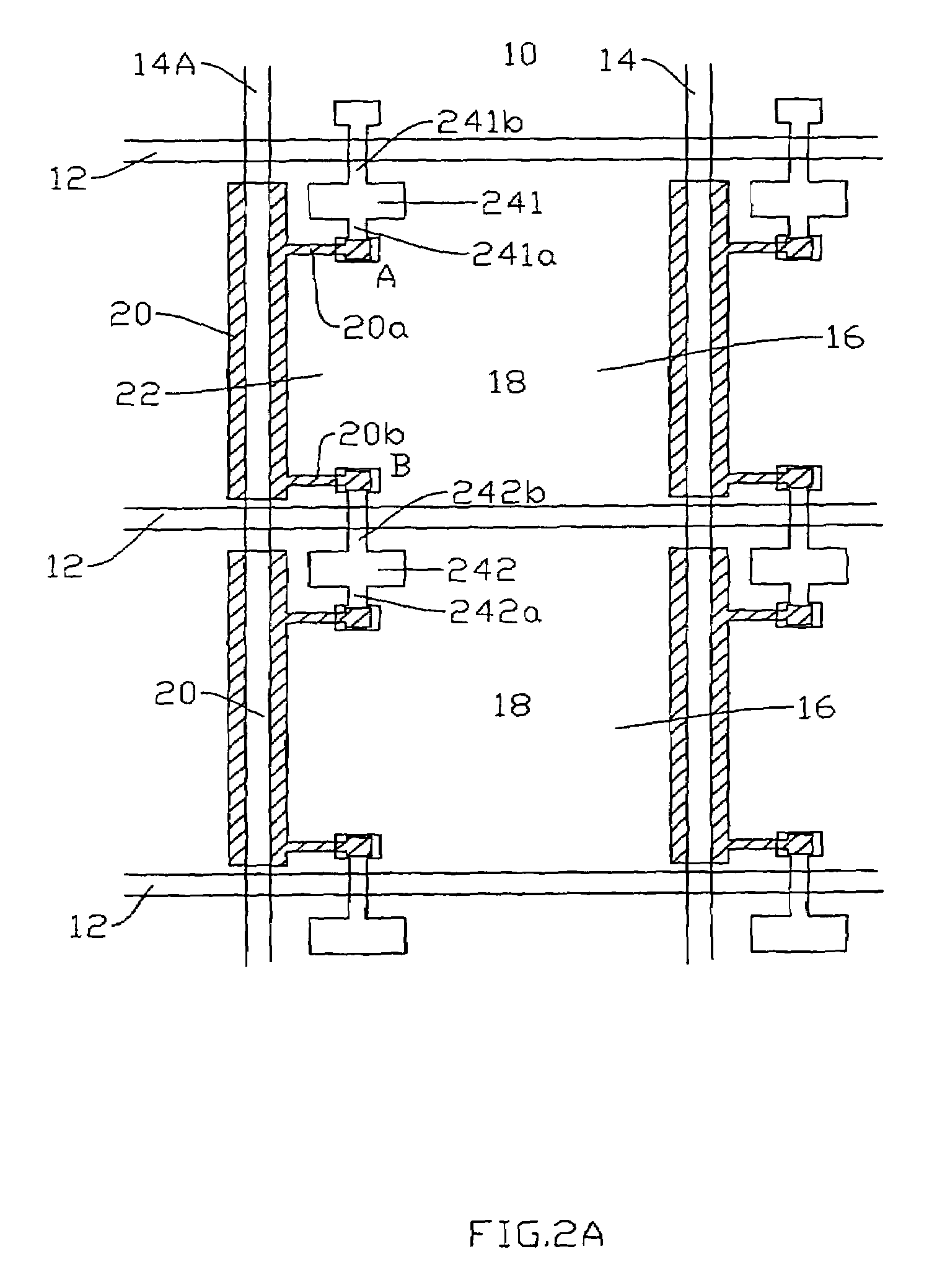
[0039]Please refer to FIG. 2A and FIG. 2B, the top view and the partially enlarging view of a laser repair structure for a transmissive LCD device according to the present invention are shown. A plurality of horizontal scan lines 12, a plurality of vertical data lines 14, and a plurality of pixel areas 16 are formed on a substrate 10 of the transmissive LCD. Each pixel area 16 is defined by two scan lines 12 and two data lines 14. A pixel electrode 18 is put on the surface of the pixel area 16 and a TFT is formed in the pixel area 16 separately. Besides, there is a pattern that floating dummy metal 20 is located between every two pixel areas and below the data lines 14 (the second metal layer) for preventing from light leakage between two pixel areas 16. The dummy metal 20 and the scan lines 12 (the first metal layer) are formed at the same time.
[0040]According to the first embodiment of the present invention, there are two extended electrical repair layers 20a-20b attached to the f...
second embodiment
[0041]Please refer to FIG. 3A and FIG. 3B, the top view and the partially enlarging view of a laser repair structure for a reflective LCD device according to the present invention are shown. A plurality of horizontal scan lines 62, a plurality of vertical data lines 64, and a plurality of pixel areas 66 are formed on the substrate 60 of the reflective LCD. Each pixel area 66 is defined by two scan lines 62 and two data lines 64. A pixel electrode 68 is put on the surface of the pixel area 66 and the TFT is formed in the pixel area 66 separately. Besides, there are a floating dummy metal 70 put in the pixel area 66 for planarizing the dielectric layer (not shown in the FIGs.). The dummy metal 70 and the scan lines 62 (the first metal layer) are formed at the same time.
[0042]According to the second embodiment of the present invention, there are two extended electrical repair layers 70a-70b attached to at least one of the floating dummy metal 70 (the first metal layer), two extended el...
PUM
| Property | Measurement | Unit |
|---|---|---|
| thickness | aaaaa | aaaaa |
| dielectric | aaaaa | aaaaa |
| width | aaaaa | aaaaa |
Abstract
Description
Claims
Application Information


