

OLED device with asymmetric host
a technology of asymmetric host and oled device, which is applied in the direction of discharge tube luminescnet screen, other domestic articles, natural mineral layered products, etc., can solve the problems that their performance limitations have represented a barrier to many desirable applications, and achieve the effect of desired operational stability
- Summary
- Abstract
- Description
- Claims
- Application Information
AI Technical Summary
Benefits of technology
Problems solved by technology
Method used
Image


Examples
example 1
Preparation of Inv-1
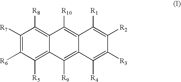
[0136]a) Preparation of 9-(4-biphenyl)anthracene. 9-Bromoanthracene (19.5 g, 75.8 mmol, 1 eq) and (1,1′-biphenyl-4-yl)boronic acid (15.0 g, 75.8 mmol, 1 eq) were combined in 100 ml of toluene and the resulting mixture degassed by sonication for about 15 min. tetrakis(triphenylphosphine) palladium (0.650 g, 0.568 mmol, 0.75%) was added and the resulting mixture was thoroughly stirred under nitrogen while 150 ml of 2M Na2CO3 were added and the mixture heated to reflux via heating mantle. The reaction was left to reflux overnight, during which time the product had precipitated out. The solid isolated by filtration and the organic phase was washed with water until the washings were neutral. The solid isolated was dissolved in hot toluene and filtered through glass fiber filter paper to remove palladium salts. The toluene phases were combined and concentrated to about 100 mL residue, which was left to recrystallize overninght. The product recrystallized was isolated b...
examples 2 , 3
EXAMPLES 2, 3
Inventive EL Devices
[0140]An EL device satisfying the requirements of the invention was constructed in the following manner:
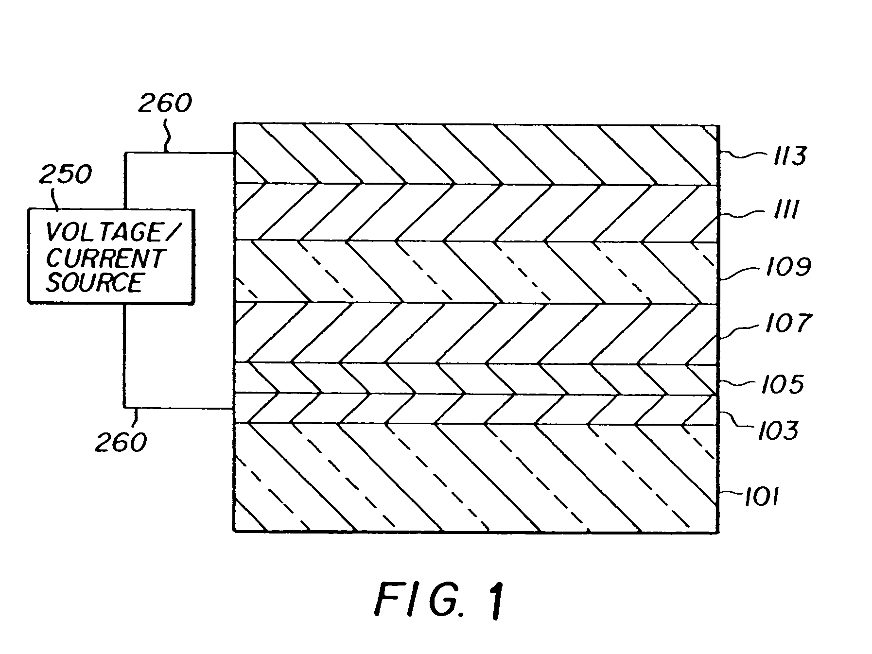
[0141]A glass substrate coated with a 42 nm layer of indium-tin oxide (ITO) as the anode was sequentially ultrasonicated in a commercial detergent, rinsed in deionized water, degreased in toluene vapor and exposed to oxygen plasma for about 1 min.[0142]a) Over the ITO was deposited a 1 nm fluorocarbon hole-injecting layer (CFx) by plasma-assisted deposition of CHF3.[0143]b) A hole-transporting layer of N,N′-di-1-naphthalenyl-N,N′-diphenyl-4, 4′-diaminobiphenyl (NPB) having a thickness of 75 nm was then evaporated from a tantalum boat.[0144]c) A 20–40 nm light-emitting layer of Inyl doped with various amounts of dopant depending upon the dopant used, was then deposited onto the hole-transporting layer. These materials were co-evaporated from tantalum boats. Herein, doping percentage is reported based on volume / volume ratio. The specific dopant, perc...
examples 4 , 5 , 6 , 7 , 8
EXAMPLES 4, 5, 6, 7, 8
Comparative EL Devices
[0148]EL devices of comparative examples were fabricated in the same manner as Example 2 except that, in place of Inv-1, other anthracene derivatives not part of this invention, were used as hosts.
[0149]
[0150]The cells thus formed in Examples 2–8 were tested for efficiency in the form of luminance yield (cd / A) measured at 20 mA / cm2. CIE color x and y coordinates were determined. It is desirable to have a luminance yield of at least about 2.2 cd / A and preferably greater than about 3 cd / A, for a blue device. The luminance loss was measured by subjecting the cells to a constant current density of 20 mA / cm2 at 70° C., or at 40 mA / cm2 at RT (room temperature), to various amounts of time that are specified for each individual cell / example. The extrapolated values are estimated based on real data at 20 mA / cm2 and 70° C., or at 40 mA / cm2 and RT. Useful stability for use in a display device is desirably less than about 40% loss after about 300 hour...
PUM
| Property | Measurement | Unit |
|---|---|---|
| thick | aaaaa | aaaaa |
| work function | aaaaa | aaaaa |
| work function | aaaaa | aaaaa |
Abstract
Description
Claims
Application Information