
Methods to form a memory cell with metal-rich metal chalcogenide

a metal-rich, memory cell technology, applied in the field of memory technology, can solve the problems of loss of data, loss of data, volatile memory data, etc., and achieve the effect of precise control and high uniformity

Inactive Publication Date: 2006-06-06
MICRON TECH INC
View PDF219 Cites 22 Cited by
  • Summary
  • Abstract
  • Description
  • Claims
  • Application Information

AI Technical Summary

Benefits of technology

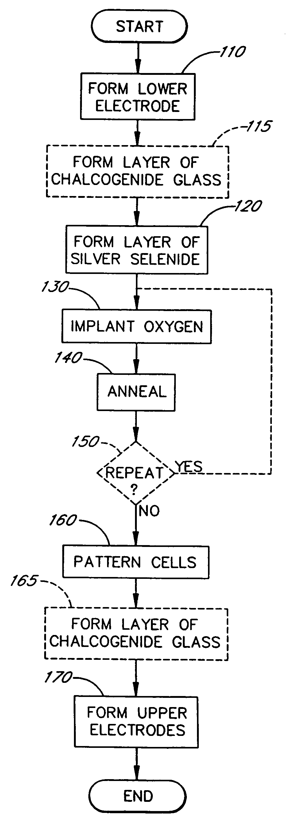
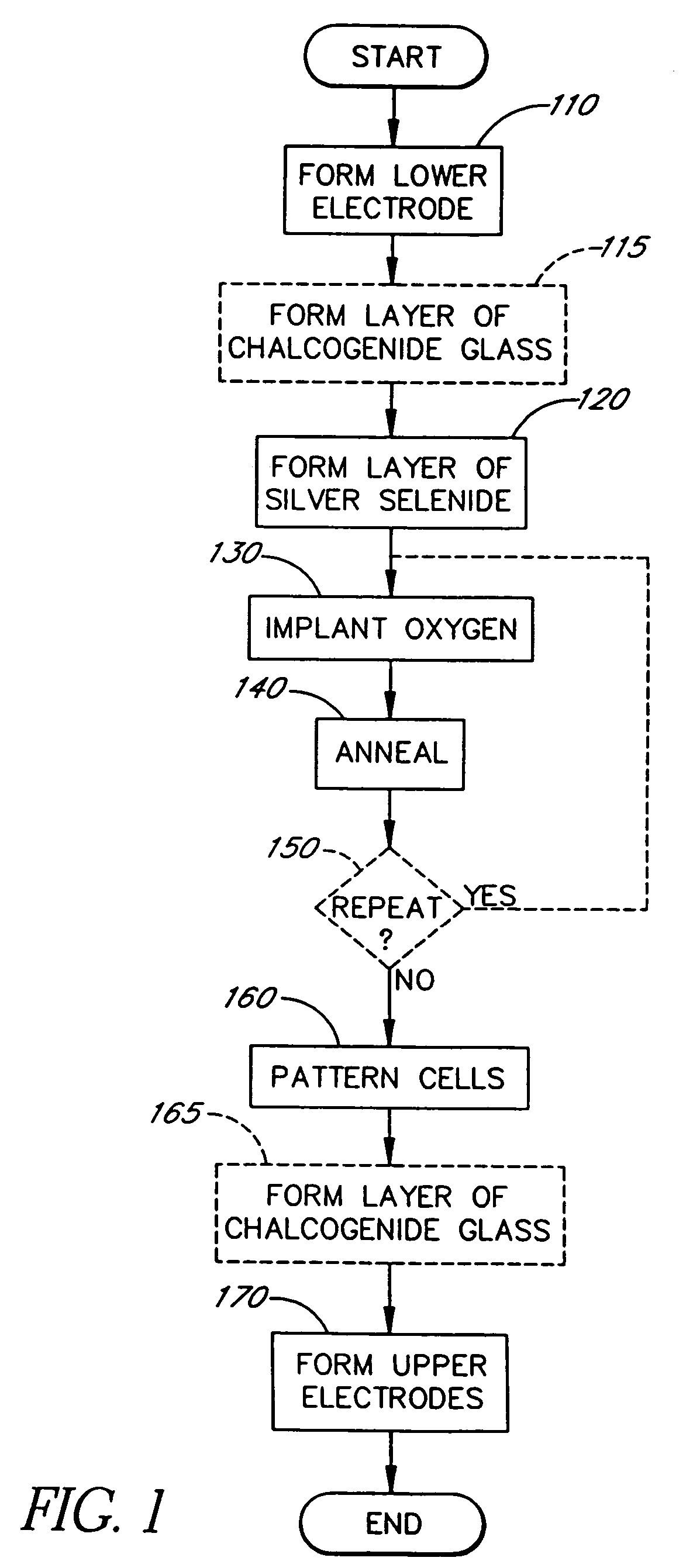
The invention describes a way to make a material called silver-rich silver selenide (Ag2+xSe) without using photodoping techniques or direct deposition of the metal. This material can be used in a resistance variable material cell. The process involves forming a layer of silver selenide, then implanting oxygen to form selenium oxide, and annealing to remove the selenium oxide. The process can be selectively enriching regions of a wafer with silver by patterning the oxygen implantation. The technical effect is the ability to make a layer of silver-rich silver selenide without using photodoping or direct deposition, which can be useful in a resistance variable material cell.

Problems solved by technology

A volatile memory loses its data when power is removed.
In addition, certain volatile memories such as DRAM devices require periodic refresh cycles to retain their data even when power is continuously supplied.
In contrast to the potential loss of data encountered in volatile memory devices, nonvolatile memory devices retain data when power is removed.
It is relatively difficult to diffuse silver uniformly across a wafer using conventional techniques.
For example, in one conventional process, the doping of the silver varies across the wafer by about 5 to 10%, which can reduce production yield.
Silver-rich silver selenide is relatively difficult to produce using direct deposition techniques.

Method used


Image

  • Methods to form a memory cell with metal-rich metal chalcogenide
  • Methods to form a memory cell with metal-rich metal chalcogenide
  • Methods to form a memory cell with metal-rich metal chalcogenide

Examples


Embodiment Construction

[0020]Although this invention will be described in terms of certain preferred embodiments, other embodiments that are apparent to those of ordinary skill in the art, including embodiments that do not provide all of the benefits and features set forth herein, are also within the scope of this invention. For example, while illustrated in the context of particular materials, the skilled artisan will appreciate that the methods described herein are applicable to doping a variety of materials with tailored amounts of metal, for a variety of applications. Accordingly, the scope of the invention is defined only by reference to the appended claims.

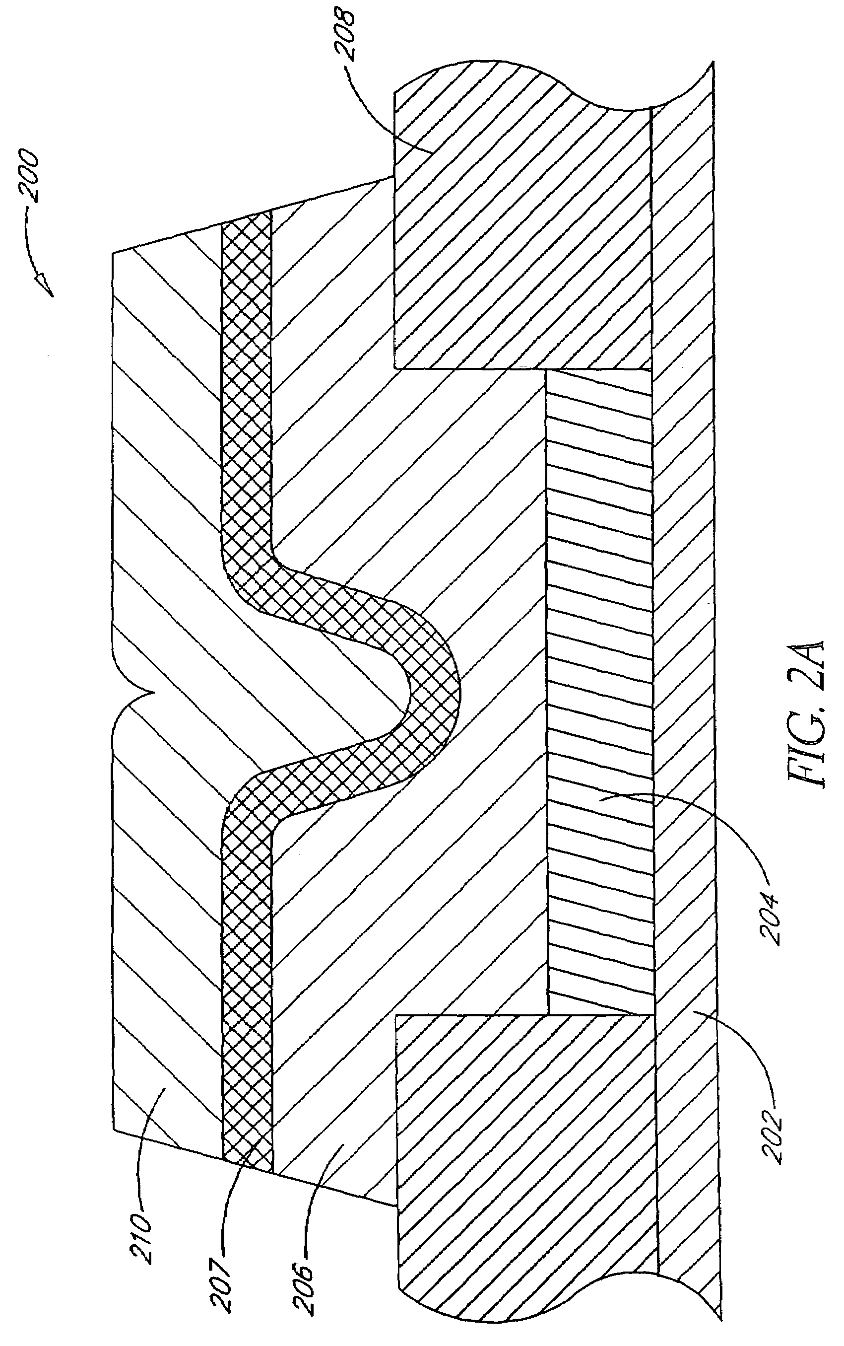
[0021]One process according to an embodiment of the invention can form silver-rich silver chalcogenide for use in a resistance variable material cell. The silver-rich silver chalcogenide cells include at least one layer of a silver-rich silver chalcogenide and at least one layer of a chalcogenide glass, such as germanium selenide (GexSe1−x). The p...


PUM

PropertyMeasurementUnit
thickaaaaaaaaaa
compositionaaaaaaaaaa
volatileaaaaaaaaaa

Abstract

The invention relates to the fabrication of a resistance variable material cell or programmable metallization cell. The processes described herein can form a metal-rich metal chalcogenide, such as, for example, silver-rich silver selenide. Advantageously, the processes can form the metal-rich metal chalcogenide without the use of photodoping techniques and without direct deposition of the metal. For example, the process can remove selenium from silver selenide. One embodiment of the process implants oxygen to silver selenide to form selenium oxide. The selenium oxide is then removed by annealing, which results in silver-rich silver selenide. Advantageously, the processes can dope silver into a variety of materials, including non-transparent materials, with relatively high uniformity and with relatively precise control.

Description

[0001]This application is a divisional of application Ser. No. 10 / 231,779 filed Aug. 29, 2002 now U.S. Pat. No. 6,867,114, which is incorporated herein by reference.BACKGROUND OF THE INVENTION[0002]1. Field of the Invention[0003]The invention generally relates to memory technology. In particular, the invention relates to memory devices with a metal-rich metal chalcogenide, such as silver-rich silver selenide.[0004]2. Description of the Related Art[0005]Computers and other digital systems use memory to store programs and data. A common form of memory is random access memory (RAM). Many memory devices, such as dynamic random access memory (DRAM) devices and static random access memory (SRAM) devices are volatile memories. A volatile memory loses its data when power is removed. In addition, certain volatile memories such as DRAM devices require periodic refresh cycles to retain their data even when power is continuously supplied.[0006]In contrast to the potential loss of data encounter...

Claims


Application Information

Patent Timeline
Patent Type & Authority Patents(United States)
IPC IPC(8): H01L21/06H01L27/24H01L45/00
CPCH01L27/2463H01L45/085H01L45/1675H01L45/1641H01L45/143H10B63/80H10N70/245H10N70/8825H10N70/041H10N70/063
Inventor MOORE, JOHN T.GILTON, TERRY L.CAMPBELL, KRISTY A.
Owner MICRON TECH INC
Learn More