Light deflection element, light deflection device and image display device

Inactive Publication Date: 2006-06-06
RICOH KK
View PDF13 Cites 6 Cited by
  • Summary
  • Abstract
  • Description
  • Claims
  • Application Information

AI Technical Summary

Benefits of technology

[0075]In addition, the above light path deflection element comprises a plurality of electrode lines that are substantially arranged parallel to a desired light path shift direction on regions containing light paths on the two substrates. Therefore, even though the effective cross-sectional area of the light path is large, the entire light path can be more uniform and effectively deflected.
[0076]The above electrode lines can be made of transparent electrode material, as seeing from the light paths, the electrode lines on each substrate are interleavedly arranged, and at a specific time, voltage values applied to the electrode lines are interleavedly and stepwise different values between the two substrates. Therefore, even though the effective cross-sectional area of the light path is large, the uniformity of the deflection amount of the entire light path can be further increased.
[0077]Furthermore, the spacers can be an electrode pair made of conductive material and located outside light path regions, the electrode lines are formed between the electrode pair with respect to the

Problems solved by technology

In general, a long optical path is necessary for obtaining a very large light deflection and applications are limited because the material is expensive.
According to the Japanese Laid-Open 9-18940, because the nematic liquid crystal is used, it is very difficult to have a response time of a sub-millisecond order, thereby it cannot be an application for a high-speed switching function.
However, because the smectic A phase liquid crystal doesn't possess a spontaneous polarization, a high-speed operation cannot be operated.
However, because the chiral element and the birefringence element are used together, there are the following problems for example.
The light loss is large and the variation of the pixel shift amount due to the wavelength of the light will reduce the resolution.
If the optical properties of the chiral element and the birefringence element are mismatched, optical noise, such as ghosting, occurs because light leakage occurs outside the pixel shift position so that the no image will be formed.
In particular, the above problem becomes obvious when the birefringence element uses materials having a large first order electro-optical (Pockels) effect, such as KH2PO4 (KDP), NH4H2PO4(ADP), LiNbO3, LiTaO3, GaAs, and CdTe etc.
However, because the image display element has to be accurately and quickly moved in parallel, the accuracy and the durability required for

Method used


Image

  • Light deflection element, light deflection device and image display device
  • Light deflection element, light deflection device and image display device
  • Light deflection element, light deflection device and image display device

Examples


first embodiment

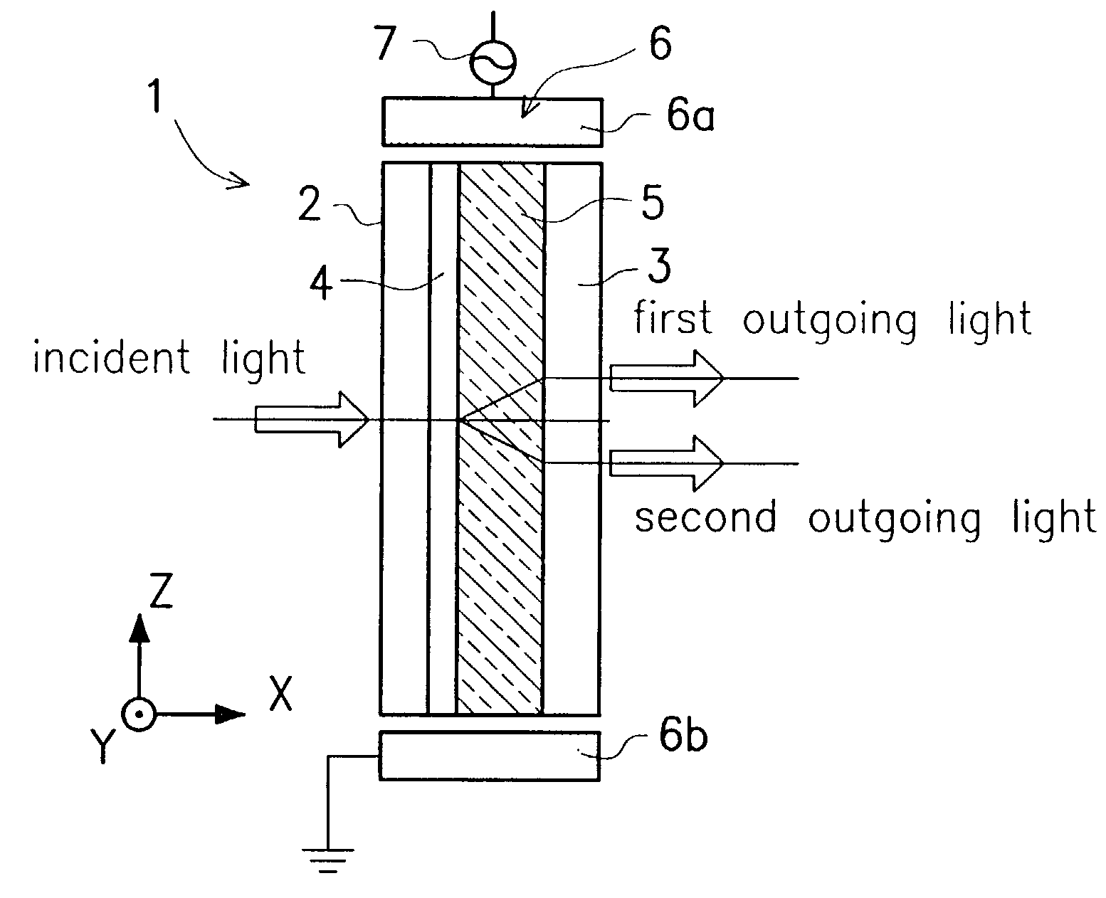
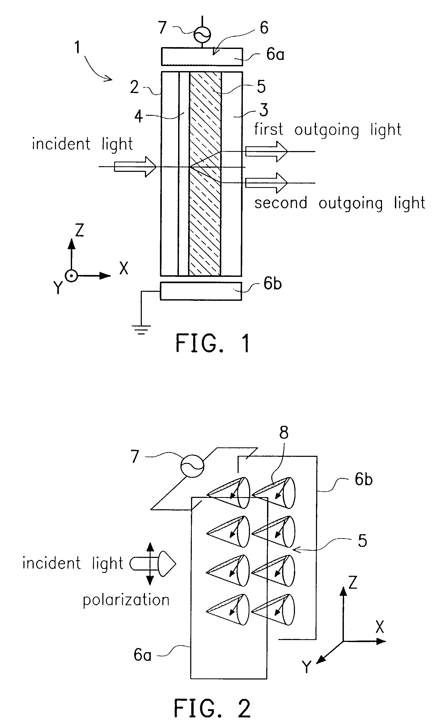
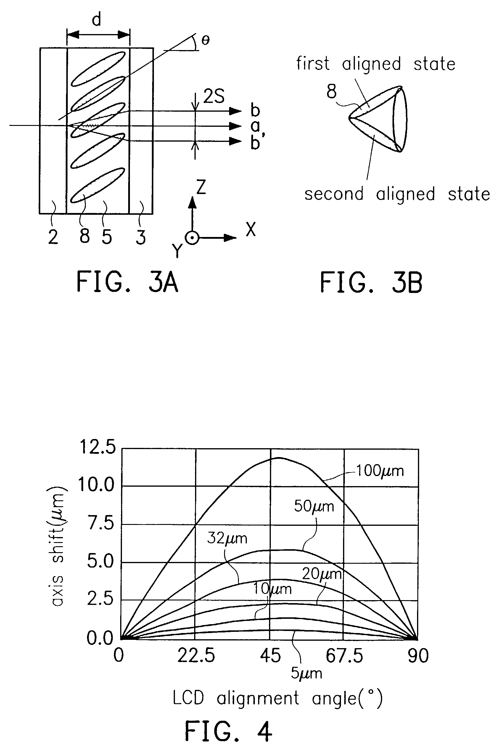
[0115]The first preferred embodiment according to the invention is described in detail with reference to FIGS. 1 to 4. FIG. 1 schematically illustrates a cross-sectional view of the structure of an optical deflecting element according to the first preferred embodiment of the invention. The optical deflecting element 1 is arranged to have a pair of transparent substrates 2, 3 that are opposite to each other. An alignment layer 4 is formed on the inner surface of one of the transparent substrates 2, 3 (here the transparent substrate 2). A ferroelectric liquid crystal (LC) 5 composed of chiral smectic C phase materials is filled between the alignment layer 4 and the other transparent substrate 3.

[0116]An electrode pair 6 consisting of electrodes 6a, 6b used for corresponding the deflecting directions of light is arranged in the above structure having the pair of transparent substrates 2, 3, the alignment layer 4 and the ferroelectric LC 5, and is connected to a power source 7. Because ...

second embodiment

[0136]The second embodiment of the invention is described in detail with reference to FIG. 5. Elements that are as same as or equivalent to the elements of the first embodiment are labeled by the same numerals, and their corresponding descriptions are omitted, which is similar to the following embodiments.

[0137]The second embodiment describes a light deflection device 10 having a structure combing two light deflection elements 1A, 1B mentioned above and a ½ wavelength plate 9. As shown in FIG. 5, the two light deflection elements 1A, 1B are respectively perpendicular to the directions of the electric fields generated by electrode pairs 6 (6a, 6b) and are arranged in series along the propagation direction of light. The ½ wavelength plate 9 is interposed between the light deflection elements 1A, 1B. The directions of electric fields generated by two electrode pairs forms a predetermined angle, for example 90 degrees.

[0138]According to the light deflection device 10, because the light ...

third embodiment

[0140]The third embodiment of the invention is described in detail with reference to FIG. 6. According to the third embodiment, in addition to the electrode pair 6, an electrode pair 11, consisting of electrodes 11a, 11b and serving as an electric field applying device for creating an electric field perpendicular to the electrode pair 6, is added to the light deflection element 1 mentioned above. A power source 12 is connected between of the electrodes 11a, 11b of the electrode pair 11. On the other hand, the electrode pairs 6, 11 are arranged in the up / down and the left / right directions with respect to the liquid crystal 5. A polarization direction switching device or a polarization direction switching device 13 is provided for controlling the deflection direction of the incident light at the incident side of the light deflection element 1 that has the electrode pairs 6, 11 above.

[0141]According to the above structure, the light deflection positions are the same as the situation in...


PUM


Abstract

A light deflection element has a pair of transparent substrates 2, 3; a chiral smectic C phase liquid crystal 5 with a homeotropic alignment filled between the pair of transparent substrates 2, 3; and at least an electric field applying device 6 for activating an electric field in the liquid crystal 5. Because a chiral smectic C phase liquid crystal is used, the problems of the conventional light deflection element, such as high cost, light loss, large size, and optical noise etc. due to its complicated structure, can be greatly improved. The conventional low response time due to the smectic A phase or the nematic liquid crystal is improved, thereby the high-speed response is possible.

Description

[0001]This is a continuation of U.S. patent application Ser. No. 10 / 052,368, filed Jan. 23, 2002, the entire disclosure of which is incorporated herein by reference.CROSS-REFERENCE TO RELATED APPLICATION[0002]This application claims the priority benefit of Japanese application serial no. 2001-285409, filed on Sep. 19, 2001 and 2001-287907, filed on Sep. 20, 2001.BACKGROUND OF THE INVENTION[0003]1. Field of the Invention[0004]This invention relates in general to a light deflection element and light deflection device that are capable of changing the propagation direction of light by electrical signals More specifically this invention relates to an image display device using the above light deflection element and light deflection device.[0005]2. Description of Related Art[0006]In the specification, a light deflection element is used for deflecting the optical path by electrical signals supplied externally. Namely, with respect to an incident light, an outgoing light is parallel shifted...

Claims


Application Information

Patent Timeline
IPC IPC(8): C09K19/02G02F1/141G02F1/29H04N5/74
CPCG02F1/133504G02F1/141G02F1/29G02F1/31H04N5/7441G02F2001/291G02F2201/124H04N5/66G02F1/291
Inventor SUGIMOTO, HIROYUKITOKITA, TOSHIAKIMATSUKI, YUMINIMURA, SHIGEAKIKOBAYASHI, MASANORITAKIGUCHI, YASUYUKIKAMEYAMA, KENJIKATOH, IKUO
Owner RICOH KK
Why Eureka
Try Eureka