Techniques for programming and verifying data in a programmable circuit

a technology of a programmable circuit and a verification circuit, applied in the direction of coding, instruments, code conversion, etc., can solve the problems of undesirably long delay time and high vector count of prior art techniques for programming and verifying data in a programmable circuit, undesirably long program and verification time delays, etc., to reduce time delays and vector counts

Inactive Publication Date: 2006-06-06
ALTERA CORP
View PDF5 Cites 56 Cited by
  • Summary
  • Abstract
  • Description
  • Claims
  • Application Information

AI Technical Summary

Benefits of technology

[0009]The present invention reduces the number of times word line address bits are loaded into the row shift registers to select word lines for programming and verifying data. Data programmed into memory cells of a first word line is verified and memory cells in a second word line are programmed for each set of address bits in the row shift registers.
[0010]The present invention also provides a technique for shifting program data bits into the column shift registers at the same time that verify data bits are shifted out of the column shift registers. This technique reduces the number of times data bits are shifted into and out of the column shift registers. By reducing the number of times bits are loaded into the row and column shift registers, the present invention reduces time delays and the vector counts associated with programming and verifying data in programmable memory circuits.

Problems solved by technology

Prior art techniques for programming and verifying data in a programmable circuit require an undesirably long delay time and a high vector count.
Loading address bits and data bits into the registers separately each time program or verify steps are performed creates a high vector count and typically causes undesirably long program and verify time delays.

Method used


Image

  • Techniques for programming and verifying data in a programmable circuit
  • Techniques for programming and verifying data in a programmable circuit
  • Techniques for programming and verifying data in a programmable circuit

Examples


Embodiment Construction

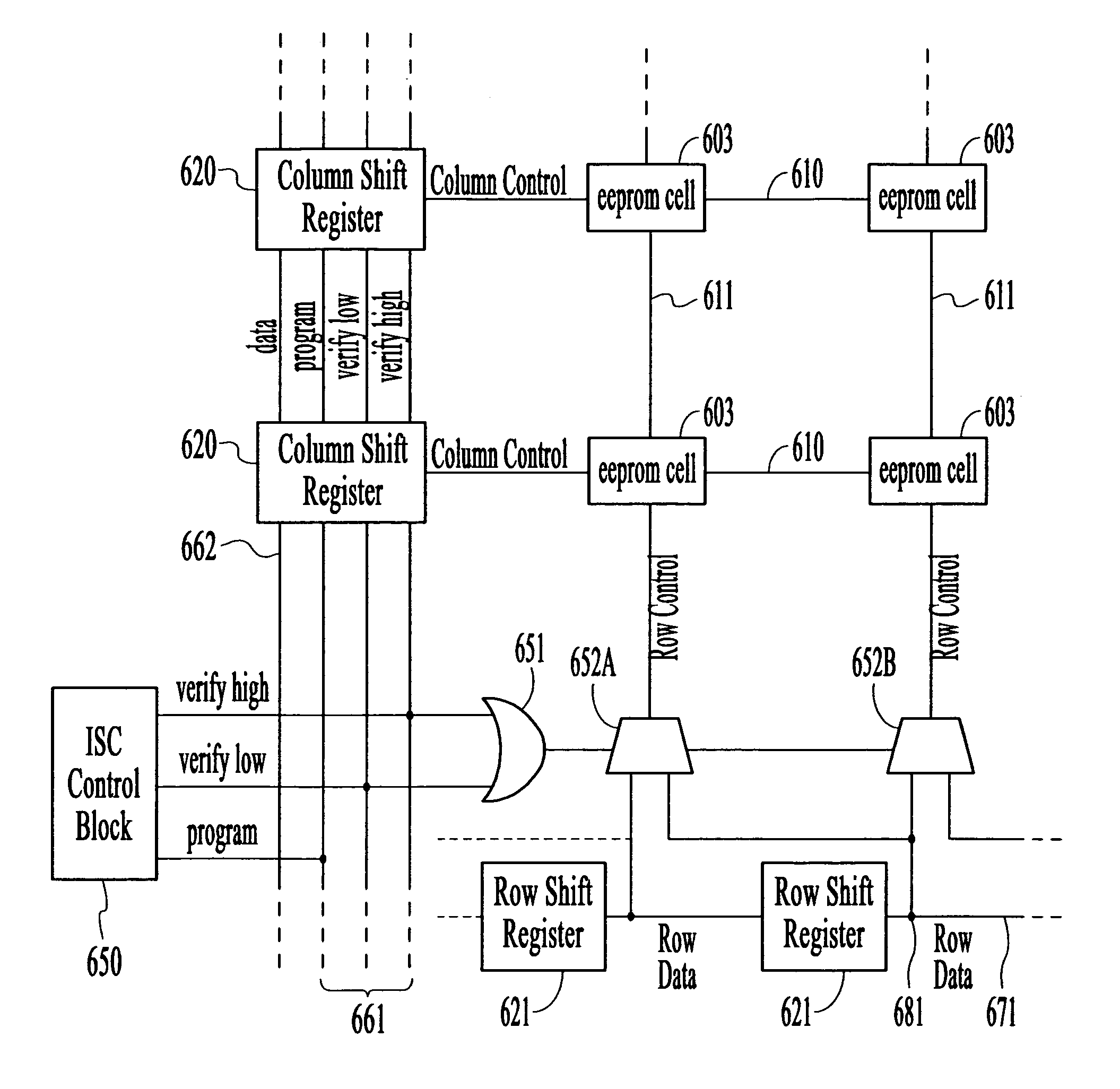
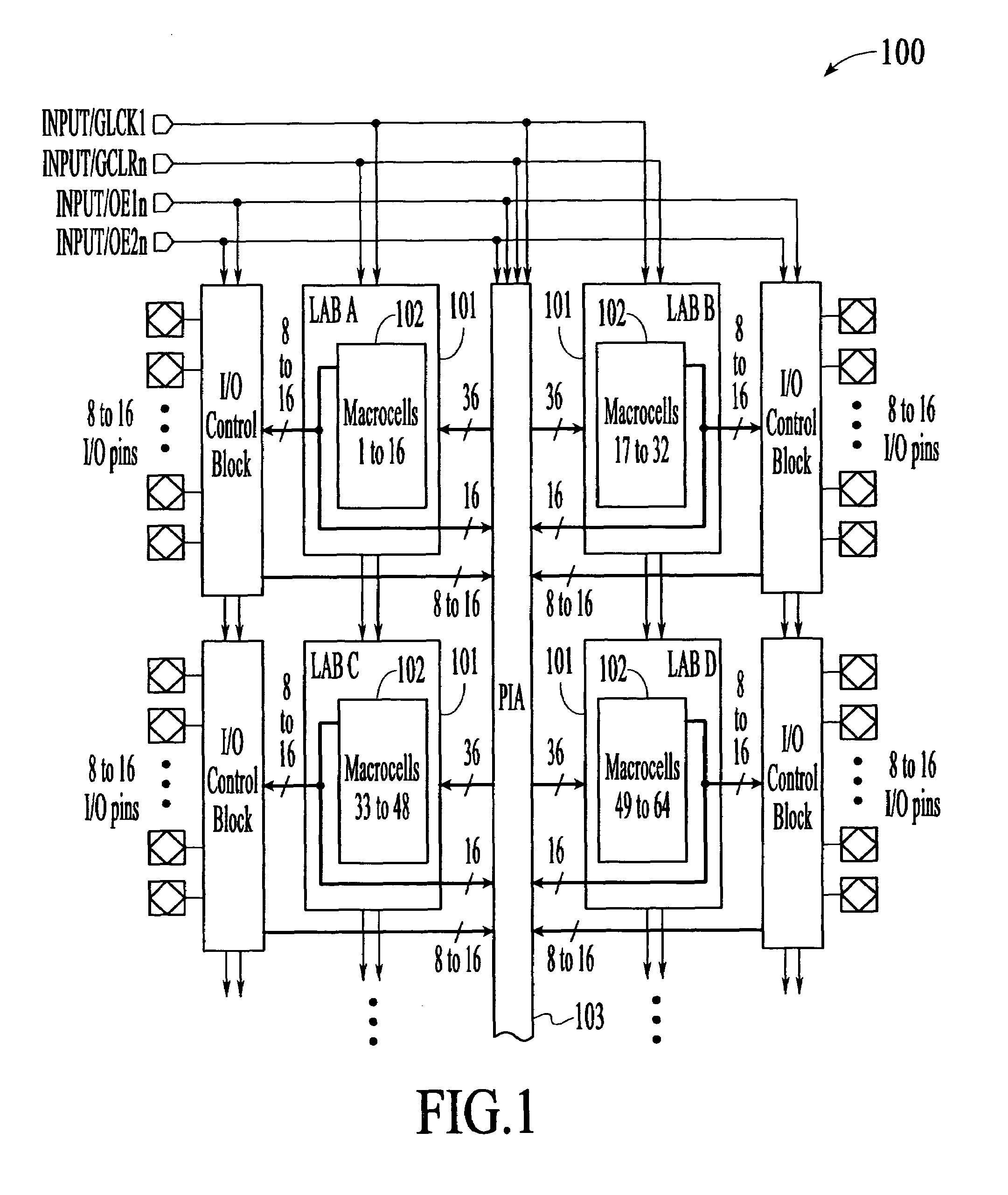
[0018]FIG. 1 illustrates a diagram of a programmable logic device (PLD) 100. PLD 100 includes a plurality of logic array blocks (LABs) 101. Programmable interconnect array 103 routes signals between LABs 101. PIA 103 includes interconnection conductors and memory elements such as EEPROM cells. Each LAB 101 includes a set of sixteen macrocells 102. Each macrocell includes a plurality of non-volatile memory cells such as EEPROM cells. The memory cells are typically arranged in a series of rows and columns. Data can be programmed into the memory cells from column shift registers (not shown).

[0019]Input and output signals can be routed between the I / O pins and the macrocells 102 via the I / O control blocks. The I / O control blocks are coupled to receive two output enable signals (OE1n and OE2n). PLD 100 also includes a clock signal GCLK1 and a clear signal GCLRn.

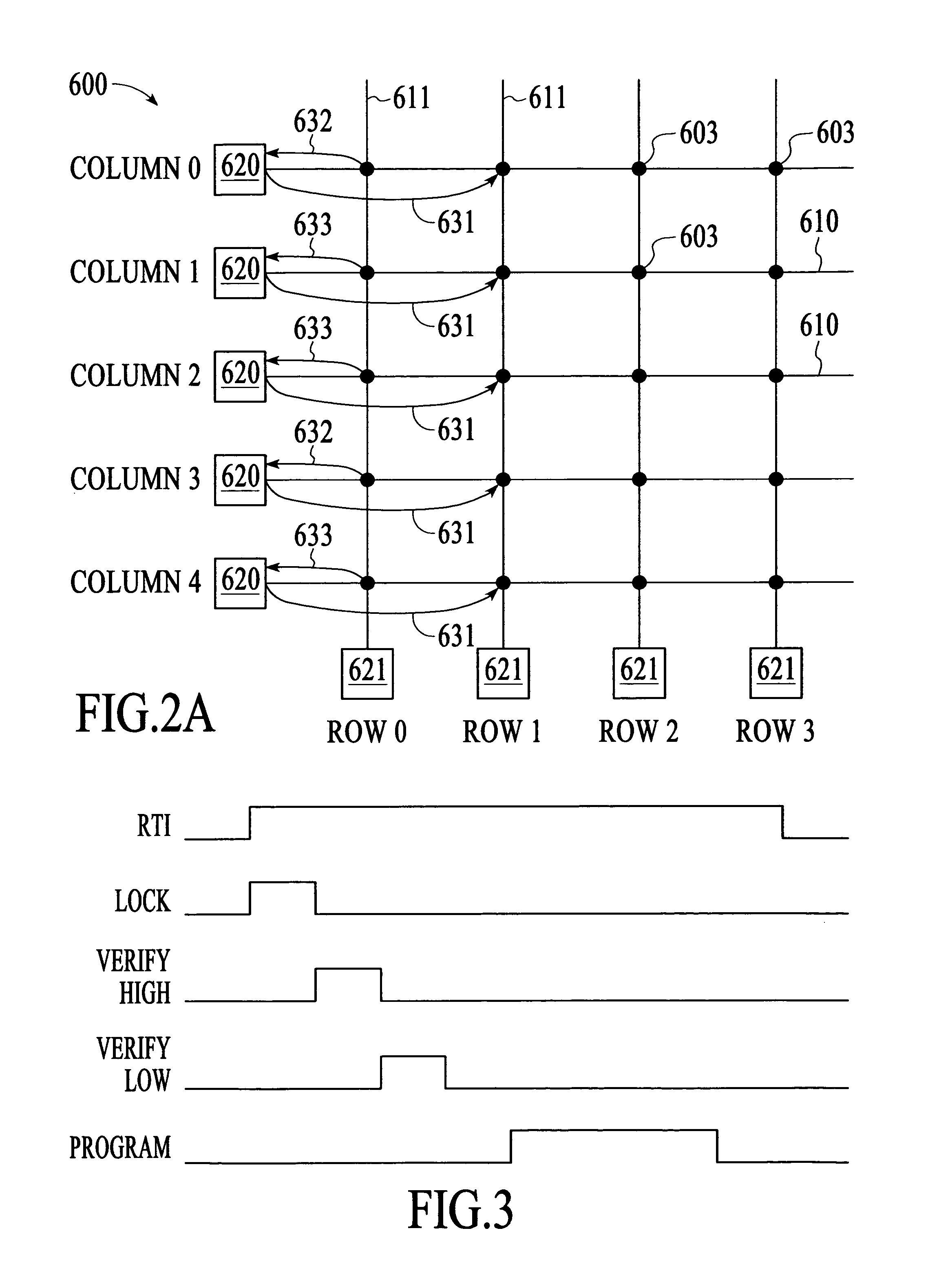
[0020]FIG. 2A illustrates a simplified diagram of a programmable circuit 600. Programmable circuit 600 may, for example, be a PL...


PUM

PropertyMeasurementUnit
delay timeaaaaaaaaaa
of timeaaaaaaaaaa
period of timeaaaaaaaaaa

Abstract

The present invention includes techniques for programming and verifying data in a programmable circuit. Programmable circuits such as PLDs may include a plurality of rows and columns of memory cells. Data is programmed into memory elements associated with the rows and columns. Subsequently, the programmed data may be extracted for verification. A first word line may be selected by first word line address bits in row shift registers. Data programmed into the first word line is loaded into column shift registers for verification during one or more verify steps. During a program step, data is programmed into memory elements in a second word line that is selected by the first word line address bits. The present invention also provides a technique for shifting program data bits into the column shift registers at the same time that verify data bits are shifted out of the column shift registers.

Description

BACKGROUND OF THE INVENTION[0001]The present invention relates to techniques for programming and verifying data in a programmable circuit, and more specifically, to techniques for programming and verifying data in a programmable circuit that saves time and reduces the vector count.[0002]Data bits can be programmed into memory cells of a programmable circuit during a program step. Subsequently, the accuracy of the data bits programmed into the memory cells can be verified during a verify step. Prior art techniques for programming and verifying data in a programmable circuit require an undesirably long delay time and a high vector count.[0003]During a program step, a first set of address bits is shifted into row shift registers that selects the word lines, and a set of program data bits is shifted into column shift registers for each word line. During a verify step, a second set of address bits is shifted into the row shift registers that selects the word lines, and verify data bits a...

Claims


Application Information

Patent Timeline
Patent Type & Authority Patents(United States)
IPC IPC(8): G06F11/00G11B5/09G11B5/00
CPCG11C16/3459G11C16/3454
Inventor DING, WEIYINGVEST, BRAD
Owner ALTERA CORP
Why Eureka
Try Eureka