Flat no-lead semiconductor die package including stud terminals

a technology of semiconductor dies and terminals, applied in the field of no-lead “packages, can solve problems such as short-circuiting caused by solder bridging

Active Publication Date: 2006-06-13
UTAC HEADQUARTERS PTE LTD
View PDF5 Cites 178 Cited by
  • Summary
  • Abstract
  • Description
  • Claims
  • Application Information

AI Technical Summary

Benefits of technology

[0007]Embodiments of this the invention can take a wide variety of forms. In some embodiments, the package is rectangular and a single row of studs are positioned on two or four sides of the package. In some embodiments two or more rows of studs can be arrayed around the die.
[0008]An epoxy layer underlying the die may be exposed on the bottom of the package, the exposed surface of the epoxy layer being substantially coplanar with the bottom surface of the capsule. In other embodiments, a plated layer of metal is exposed on the bottom of the package. In still other embodiments, the die is attached to a die-attach pad, which is exposed on the bottom of the package. Bonding wires may extend from the die to the die-attach pad. The die-attach pad can protrude from the bottom surface of the capsule such ...

Problems solved by technology

Another problem that can occur is short-circuiting resulting from sol...

Method used


Image

  • Flat no-lead semiconductor die package including stud terminals
  • Flat no-lead semiconductor die package including stud terminals
  • Flat no-lead semiconductor die package including stud terminals

Examples


Embodiment Construction

[0052]To illustrate the breadth of this invention, a variety of packages and processes for fabricating the packages will be described.

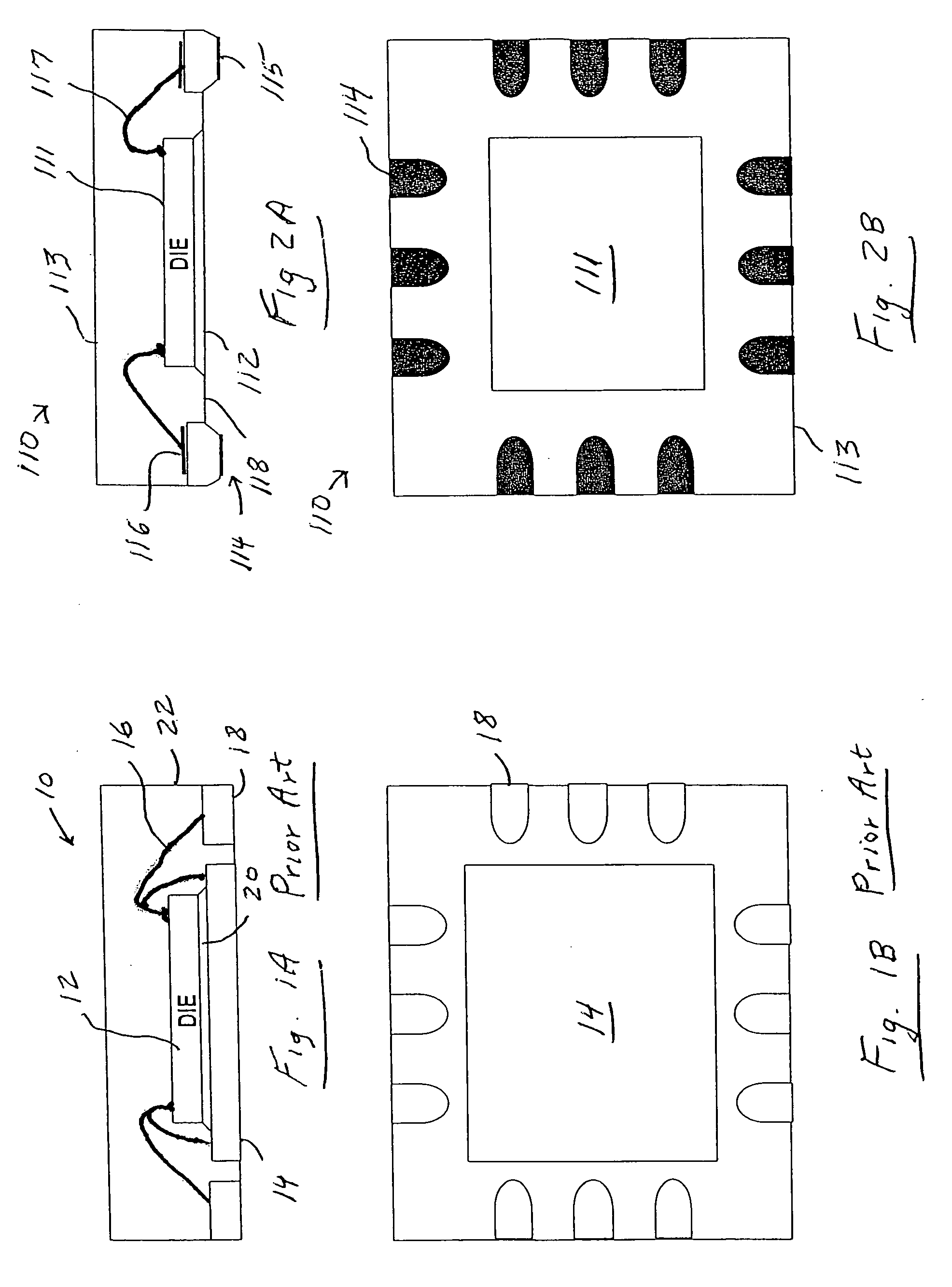
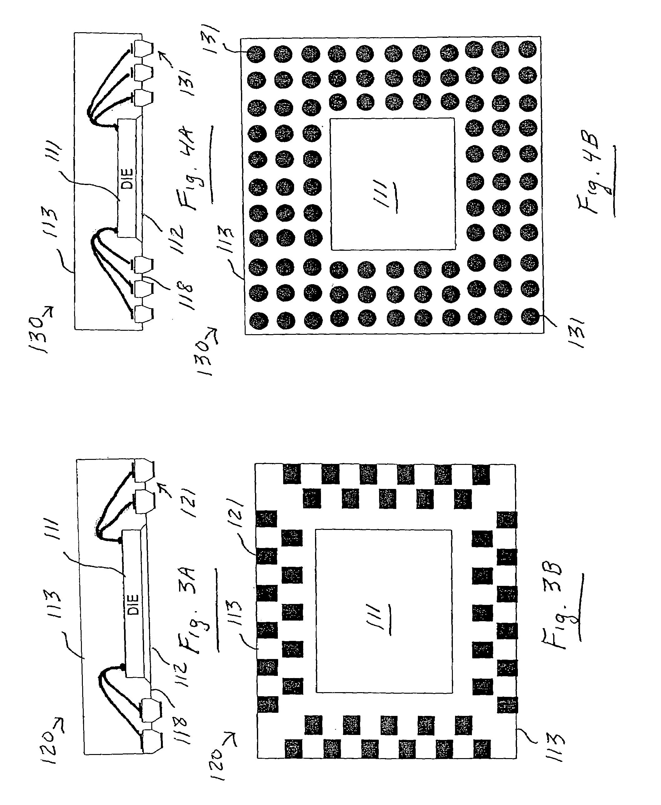
[0053]FIGS. 2A, 3A and 4A are cross-sectional views of packages 110, 120 and 130, respectively. Bottom views of packages 110, 120 and 130 are shown in FIGS. 2B, 3B and 4B, respectively.

[0054]Referring first to FIGS. 2A and 2B, package 110 includes a semiconductor die 111, which is enclosed in a capsule 113. Capsule 113 is normally made of a plastic molding compound. The molding compound may be a polymer or other epoxy material such as the Sumitomo G600 series, G770 series, EME 7730 series or the Hitachi CEL 9200 series, CEL 9220, CEL 9840 series, etc. Underlying die 111 is an exposed layer of epoxy 112, which is substantially coplanar with the bottom surface 118 of capsule 113. As shown in FIG. 2B, a plurality of metal studs 114 are positioned along the lateral edges of package 110. Referring again to FIG. 2A, studs 114 protrude from the bottom surfac...


PUM


Abstract

A flat no-lead semiconductor die package contains a plurality of studs that protrude from the bottom surface of the capsule and act as electrical contacts, allowing the package to be mounted on a flat surface such as a printed circuit board, while permitting external circuit to be located on the flat surface directly beneath the package. The package may or may not contain a die-attach pad. The die may be mounted flip-chip style on the stud contacts and die-attach pad. A method of fabricating the package includes etching an upper portion of a metal sheet through a mask layer, attaching dice at locations on the surface of the metal sheet, forming a layer of molding compound over the dice, etching the lower portion of the metal sheet through a second mask layer, and separating the packages with a dicing saw or punch tool.

Description

FIELD OF THE INVENTION[0001]This invention relates to packages for semiconductor dice and in particular to “no-lead” packages, i.e., packages in which there are no leads protruding from the surfaces of the package. Instead, electrical contact to external circuitry is made by means of contacts having exposed faces that are flush with the surfaces of the package.BACKGROUND OF THE INVENTION[0002]Semiconductor dice are normally packaged in a plastic capsule to protect them from physical damage. Connections are made to external circuitry, such as a printed circuit board (PCB), by means of sheet metal pieces, called “lead fingers,” that protrude from the capsule and can be soldered or otherwise connected electrically. Alternatively, in a “no lead” package the external connections are made in other ways, e.g., by means of contacts having faces that are flush with the surfaces of the capsule. Two types of “no-lead” packages are designated in the industry as QFN (Quad Flat No Lead) and DFN (...

Claims


Application Information

Patent Timeline
IPC IPC(8): H01L21/44
CPCH01L21/4832H01L23/3107H01L24/97H01L21/561H01L24/48H01L2224/16245H01L2224/32245H01L2224/32257H01L2224/48091H01L2224/48247H01L2224/48257H01L2224/73265H01L2224/83001H01L2224/85001H01L2224/97H01L2924/01029H01L2924/01046H01L2924/01047H01L2924/01078H01L2924/01079H01L2924/01082H01L2924/18165H01L2924/19041H01L2924/19043H01L2224/48137H01L2924/01033H01L2924/01006H01L2224/85H01L2924/00014H01L2224/83H01L2224/81H01L2924/00H01L2924/00012H01L2924/181H01L24/73H01L2224/49109H01L24/49H01L2924/00011H01L2224/49433H01L2224/0401H01L2224/45099H01L2224/45015H01L2924/207
Inventor SIRINORAKUL, SARAVUTHNONDHASITTHICHAI, SOMCHAIJEWJAITHAM, SITTA
Owner UTAC HEADQUARTERS PTE LTD
Why Eureka
Try Eureka