Liquid crystal device, liquid crystal display panel and method for manufacturing the same

a liquid crystal display panel and liquid crystal technology, applied in non-linear optics, instruments, optics, etc., can solve problems such as leakage current, and achieve the effects of avoiding concave etching stoppers, precise alignment, and long tim

Inactive Publication Date: 2006-06-13
IBM CORP +1
View PDF9 Cites 2 Cited by
  • Summary
  • Abstract
  • Description
  • Claims
  • Application Information

AI Technical Summary

Benefits of technology

[0017]Moreover, in the method of manufacturing a liquid crystal display panel, after the aforementioned steps, a source / drain layer is formed. Then, the source / drain layer and a remaining portion of the etching stopper are etched through chemical gas phase etching by photolithography. This manufacturing method makes it possible to eliminate a concave of the etching stopper, which is formed in the channel width direction as a result of excessive over-etching, and therefore, a leakage current can be prevented from flowing between the source electrode and the drain electrode.
[0018]In the liquid crystal device, the liquid crystal display panel and the method for manufacturing them according to the present invention, exposure of an etching stopper layer includes merely one exposure process using a gate electrode as a light shielding mask. Thus, the number of exposure processes in this invention is smaller by one than that of the conventional technique. Since the method of the present invention does not include the exposure process using a light-shielding mask such as a reticle, which requires preciseness in alignment and takes a long time, the productivity can be remarkably improved.
[0019]In addition, a resist for forming the etching stopper is formed on the entire gate electrode and has a larger adhesion area than that used in the conventional technique. Therefore, the photoresist is less likely to peel off, and hence, the occurrence of formation failures of the resist can be suppressed, and the failure of transistors can be reduced. Furthermore, the manufacturing cost can be largely decreased because an expensive reticle is not necessary.
[0020]In the manufacturing method of the present invention, an etching stopper which is longer in the channel width direction than the width of a source / drain electrode under layer is formed through an exposure process from the back surface side of a substrate and an exposure process from the front surface thereof Therefore, a reticle and another light-shielding mask used in the exposure process from the front surface of the substrate can be merely roughly aligned. As a result, not only the workability involved in the alignment can be remarkably improved but also the occurrence of failures can be largely reduced and the device quality can be stabilized.
[0021]Furthermore, the etching stopper longer in the channel width direction than the width of the source / drain electrode under layer is removed at its ends through etching simultaneously with the formation of the source / drain electrode under layer. Therefore, a resist used for forming the source / drain electrode under layer can be very easily aligned, and the occurrence of failures involved in the alignment can be substantially avoided.
[0022]Moreover, since the etching stopper longer in the channel width direction is etched at its ends simultaneously with the formation of the source / drain electrode under layer, even when over-etching in the etching of the etching stopper layer is so excessive that a concave in an oppositely tapered shape is formed, the concave extending over a source electrode and a drain electrode can be removed through etching. As a result, no leakage current flows between the source electrode and the drain electrode, and the performance and the quantity can be improved. In addition, since the concave formed through the excessive over-etching can be thus removed, resultant products can be used as good products. Thus, the occurrence of failure can be largely reduced.

Problems solved by technology

When a side surface extending along current flow is oppositely tapered, a leakage current can be caused owing to a remaining impurity and the like.

Method used


Image

  • Liquid crystal device, liquid crystal display panel and method for manufacturing the same
  • Liquid crystal device, liquid crystal display panel and method for manufacturing the same
  • Liquid crystal device, liquid crystal display panel and method for manufacturing the same

Examples


Embodiment Construction

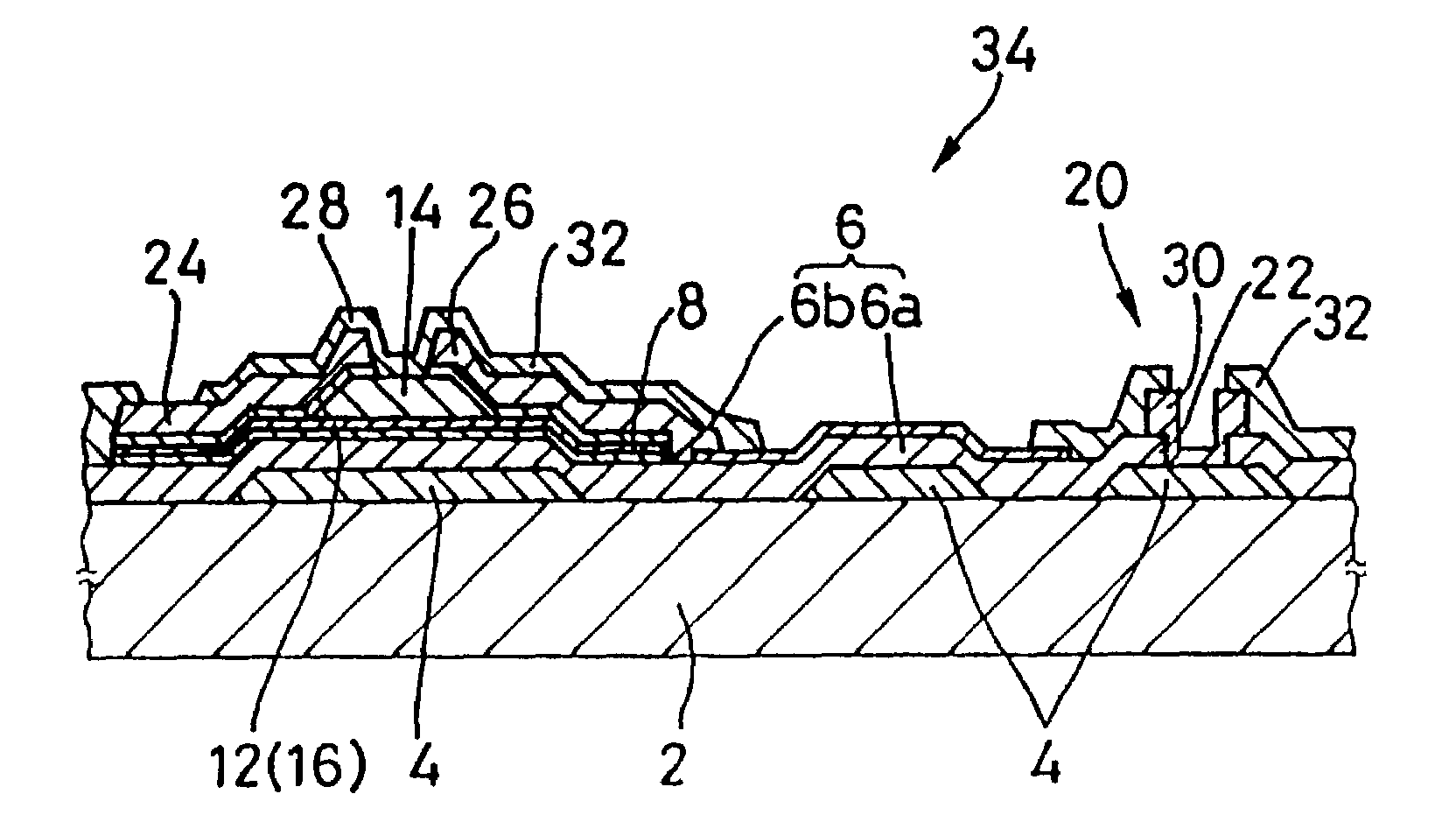
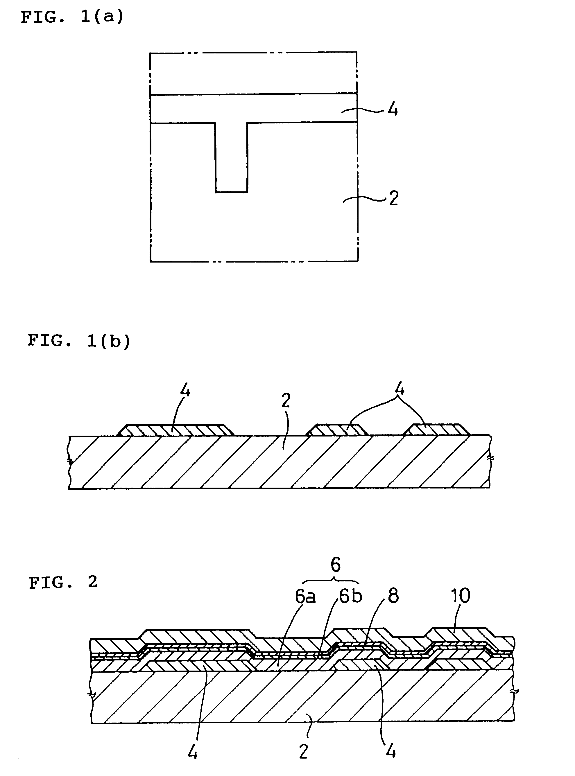
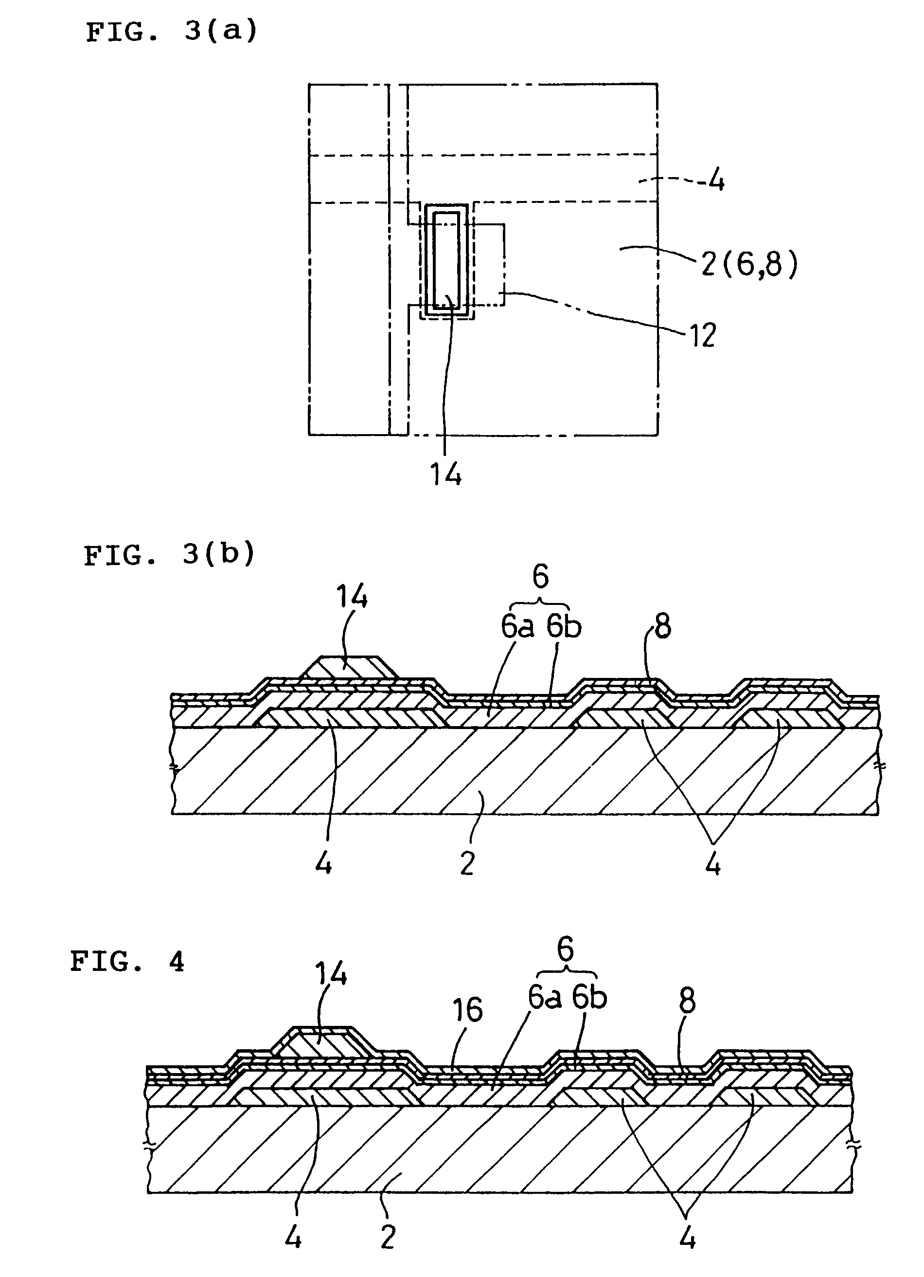
[0041]Now, a preferred embodiment of a liquid crystal device, a liquid crystal display panel and a method of manufacturing the device and the display panel will be described with reference to the accompanying drawings. It is noted that only a portion corresponding to one pixel is shown in the drawings for simplification. In addition, the sectional views illustrate, in principle, a TFT portion, a storage capacitance portion Cs and a pad portion for simplifying the description.

[0042]As shown in FIGS. 1(a) and 1(b), a gate electrode 4 (to be connected to a gate line in practice) is first formed on a transparent substrate 2. The most preferable transparent substrate 2 is a glass substrate, but can be a resin substrate or a flexible substrate as far as it is transparent and, in particular, good at heat resistance.

[0043]The gate electrode 4 consists of one or more layers of at least one element selected from the group consisting of MoW, Cr, Cu, Ni, Al, Mo, Ag and the like. Preferably, the...


PUM

PropertyMeasurementUnit
widthaaaaaaaaaa
currentaaaaaaaaaa
shapeaaaaaaaaaa

Abstract

A method of manufacturing a liquid crystal panel comprises the steps of forming a gate insulating film, a channel layer and an etching stopper layer on a transparent substrate bearing a gate electrode, exposing the substrate to light from its back surface side by using the gate electrode as a light shielding mask by photolithography, developing the resist, etching the etching stopper layer, forming a source/drain layer, and etching the source/drain layer and a remaining part of the etching stopper by chemical gas phase etching.

Description

[0001]This is a divisional of U.S. Ser. No. 09 / 409,266 filed Sep. 30, 1999 now U.S. Pat. No. 6,465,285, the contents of which are incorporated herein in its entirety.BACKGROUND OF THE INVENTION[0002]1. Field of the Invention[0003]The present invention relates to an a-Si TFT liquid crystal device, a liquid crystal display panel and a method of manufacturing them.[0004]2. Description of Related Art[0005]A conventional method for manufacturing an a-Si TFT liquid crystal display panel will now be described with regard to one liquid crystal device portion. As shown in FIGS. 15(a) and 15(b), a gate electrode 4 is first formed into a predetermined shape on a glass substrate 2 by a general technique. Then, as shown in FIG. 16, a gate insulating film 6, a channel layer 8 and a SiNx film 10 serving as an etching stopper layer are successively stacked on the entire surface of the glass substrate 2. As shown in FIGS. 17(a), 17(b) and 17(c), after coating a resist on the SiNx film 10, the glass ...

Claims


Application Information

Patent Timeline
Patent Type & Authority Patents(United States)
IPC IPC(8): H01L29/04G02F1/1343G02F1/136G02F1/1368H01L21/336H01L29/49H01L29/786
CPCG02F1/1368H01L29/78633H01L29/66765H01L29/78609G02F2001/136231H01L29/4908G02F1/136231G02F1/1343
Inventor TOKUHIRO, OSAMUUEDA, HIROYUKIMACHIDA, MASAHIKO
Owner IBM CORP
Why Eureka
Try Eureka