

Bump layout on silicon chip
a silicon chip and layout technology, applied in semiconductor devices, electrical equipment, semiconductor/solid-state device details, etc., can solve the problems of uneven stress and low reliability of the assembled structure, and achieve the effect of avoiding the lightening of the shorter side of the conventional rectangular drive chip, facilitating the placement of more bumps, and optimizing the pressure distribution
- Summary
- Abstract
- Description
- Claims
- Application Information
AI Technical Summary
Benefits of technology
Problems solved by technology
Method used
Image

Examples
Embodiment Construction
[0022]Reference will now be made in detail to the present preferred embodiments of the invention, examples of which are illustrated in the accompanying drawings. Wherever possible, the same reference numbers are used in the drawings and the description to refer to the same or like parts.
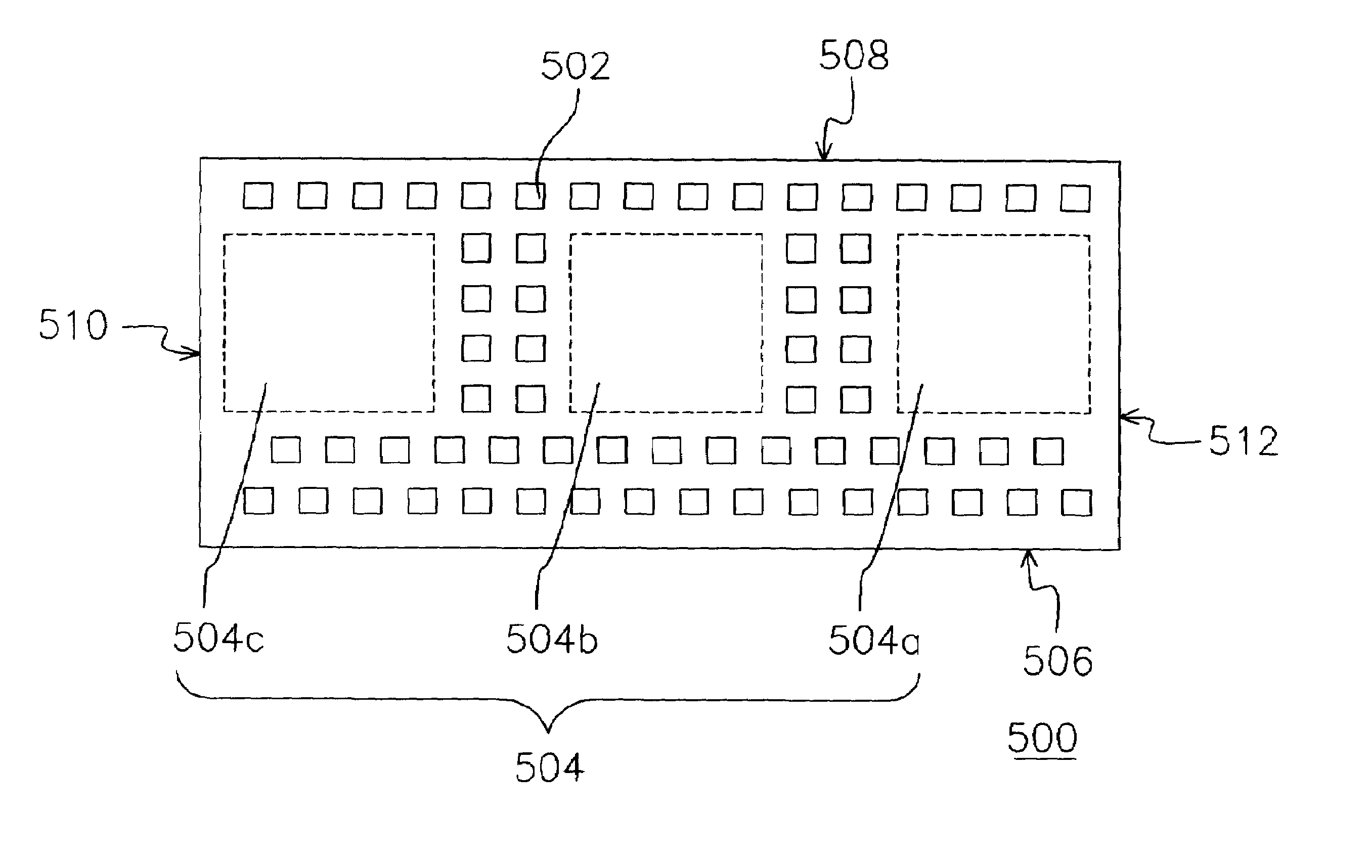
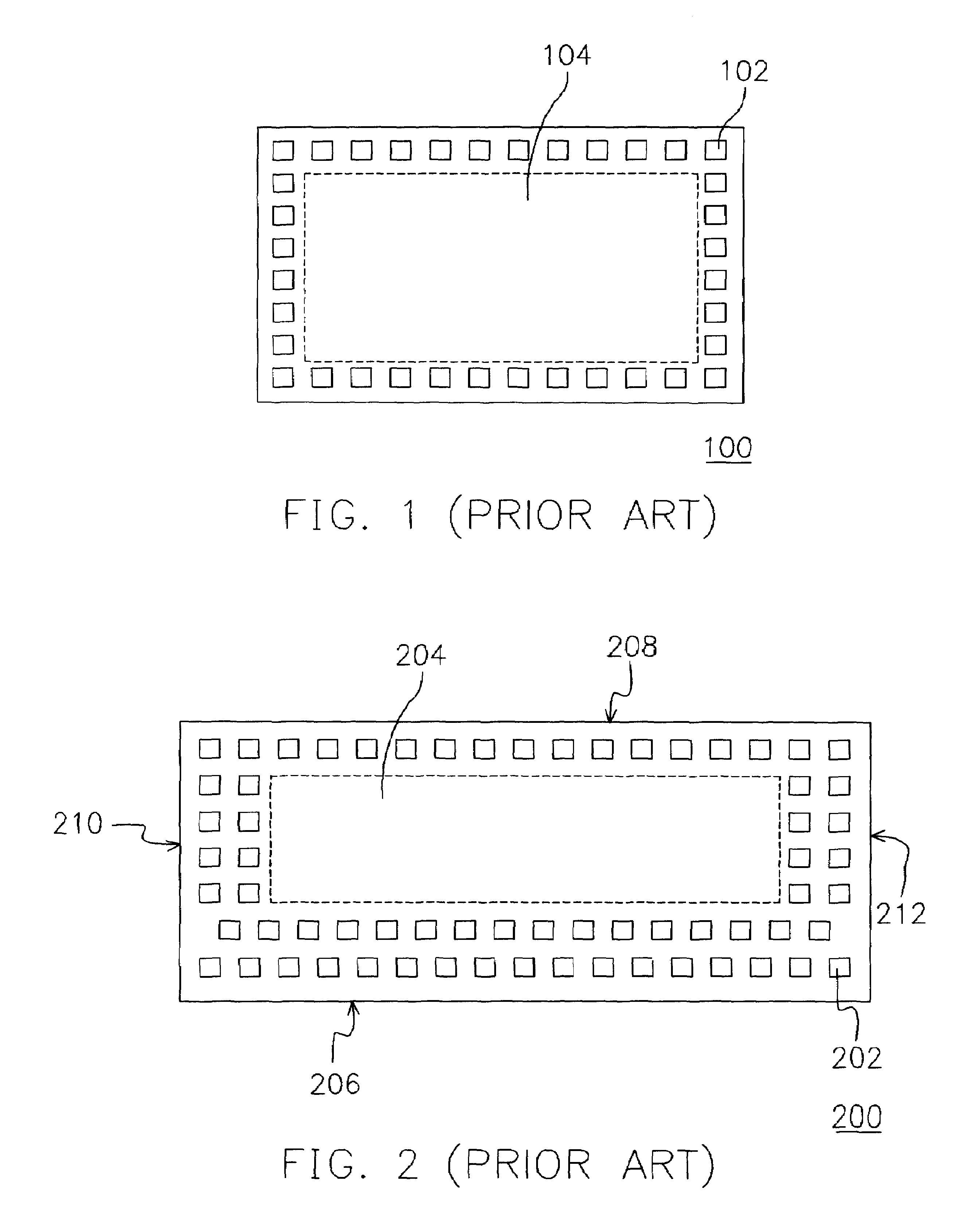
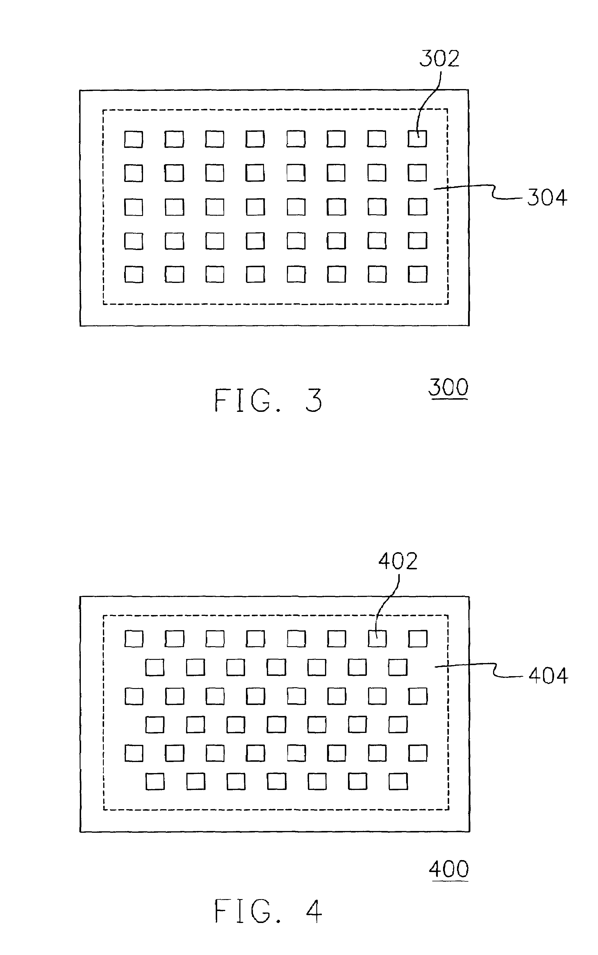
[0023]FIGS. 3 and 4 are top views showing two alternative bump layouts of a driver IC according to a first preferred embodiment of this invention. To match the ever-increasing demand for input / output (I / O) terminals in a driver IC package, the driver IC 300 of this invention is able to provide more bumps 302 in the active region. As shown in FIG. 3, the bumps 302 are positioned to form a grid array in the active region. The bumps are arranged, for example, to form a vertically aligned grid over the active region so that pressure is evenly distributed during chip-on-glass (COG) manufacturing. Circuit regions 304 are formed underneath bump space between neighboring bumps. Thus, surface area of the driv...
PUM
 Abstract
Description
Claims
Application Information