

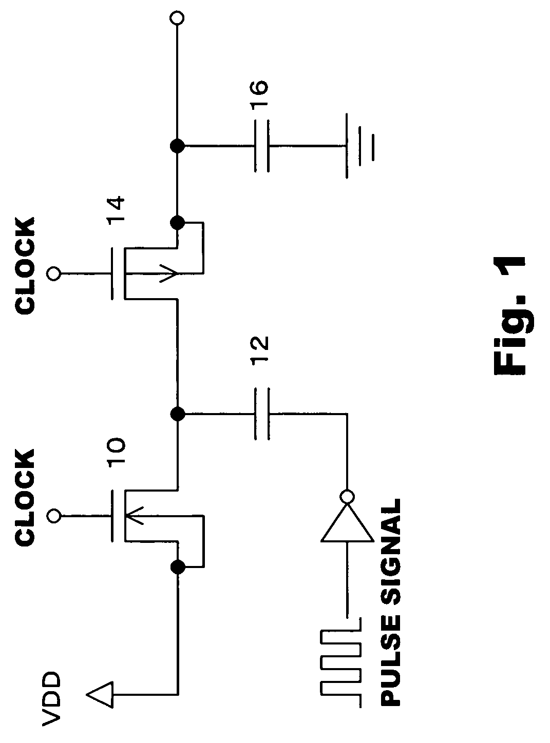
Constant current circuit used for ring oscillator and charge pump circuit
a constant current circuit and charge pump technology, applied in pulse generators, instruments, pulse techniques, etc., can solve the problems of large amount of source current consumed in vain, large amount of source current output, and source voltage, so as to avoid unnecessary consumption of a large amount of source curren
- Summary
- Abstract
- Description
- Claims
- Application Information
AI Technical Summary
Benefits of technology
Problems solved by technology
Method used
Image

Examples
Embodiment Construction
[0017]Referring to drawings, an example structure according to an embodiment of this invention will be described.
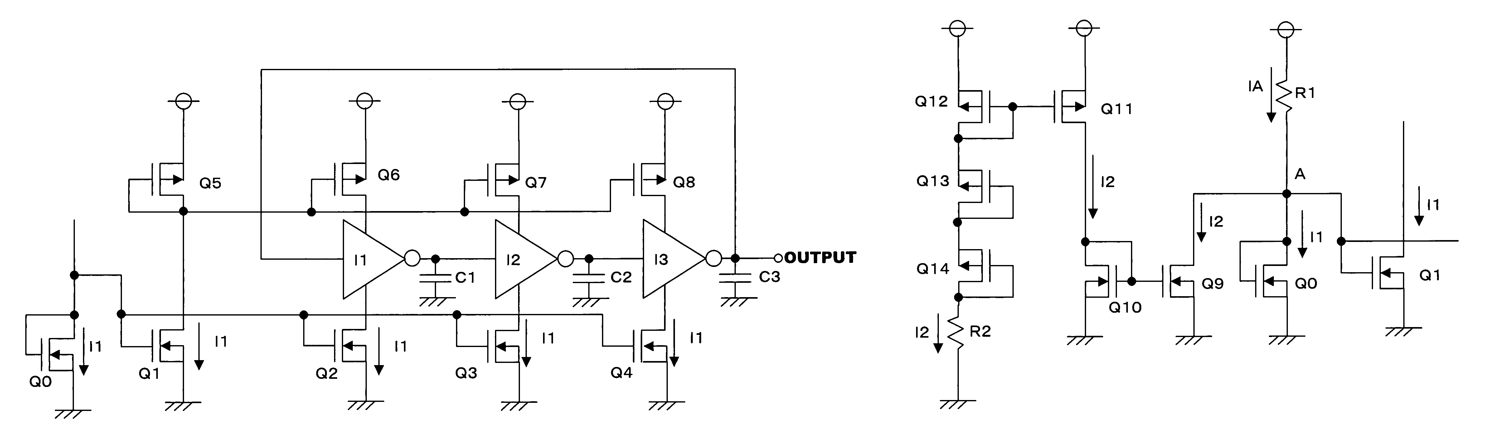
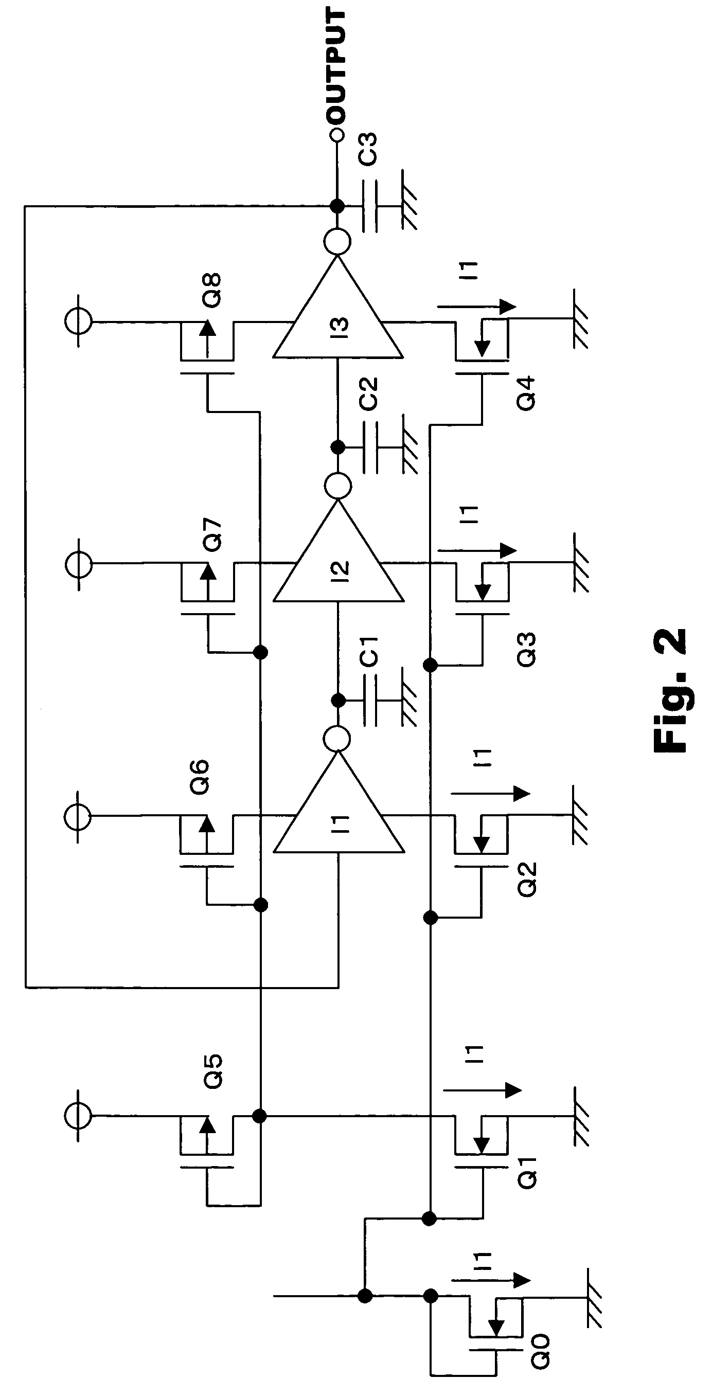
[0018]FIG. 2 shows the structure of a ring oscillator. In this structure, three inverters IV1, IV2, and IV3 are connected in series shaped like a ring. Each output of the inverters IV1, IV2, and IV3 is individually connected to one of capacitors C1, C2, and C3 which are connected to ground at the other terminals. A clock is output from the output of the inverter C3 and supplied to a charge pump circuit.
[0019]A gate of an N channel transistor (NMOS) Q0 with a short circuit between the gate and the drain in which a predetermined set current I1 flows is connected to gates of N channel transistors Q1, Q2, Q3, and Q4 whose sources are connected to ground. The current I1 runs through all the transistors Q0 to Q4. The transistors Q2, Q3, and Q4 determine operation currents for the inverters IV1, IV2, and IV3. A drain of the transistor Q1 is connected to a drain of a P channel tr...
PUM
 Abstract
Description
Claims
Application Information