Light emitting module and method of driving the same, and optical sensor

a technology of light emitting modules and optical sensors, applied in static indicating devices, photometry using electric radiation detectors, instruments, etc., can solve the problems of reducing life, increasing power consumption, and reducing power consumption, so as to reduce power consumption, improve visibility, and reduce brightness

Inactive Publication Date: 2006-06-27
SEMICON ENERGY LAB CO LTD
View PDF61 Cites 109 Cited by
  • Summary
  • Abstract
  • Description
  • Claims
  • Application Information

AI Technical Summary

Benefits of technology

[0011]A light emitting module in accordance with the present invention is characterized in that it includes a sensor section to sense the illuminance of an environment where the light emitting module is used (hereinafter referred to as environmental illuminance) and means for adjusting the luminance of a light emitting element according to the environmental illuminance and for keeping the ratio of the luminance of the light emitting element to the environmental illuminance (contrast ratio between the luminance of the light emitting element and the environmental illuminance) at a constant value.
[0012]In other words, the light emitting module in accordance with the present invention is characterized in that the luminance of an EL element can be increased in a bright use environment to improve visibility and that the luminance of the EL element can be decreased in a dark use environment to reduce power consumption without degrading visibility.
[0015]The light emitting module in accordance with the present invention is excellent in visibility in a bright environment because of a sufficiently bright display and reduces power consumption in a dark environment because it is possible to decrease brightness to a minimum while ensuring good visibility. Therefore, an electric appliance employing the light emitting module in accordance with the present invention has excellent visibility in a display section and can reduce power consumption.

Problems solved by technology

The passive type light emitting device has an advantage that it has a simple structure which reduces manufacturing costs, but it has a problem that as the pixel is of higher definition (the number of pixels increases), the luminous intensity of the EL element needs to be increased, that is, a larger current is required with results of an increase in power consumption and a reduction in life.
However, because the active matrix type light emitting device is driven by a current, it is required to decrease the power consumption.

Method used


Image

  • Light emitting module and method of driving the same, and optical sensor
  • Light emitting module and method of driving the same, and optical sensor
  • Light emitting module and method of driving the same, and optical sensor

Examples


embodiments

(Embodiments)

(Embodiment 1)

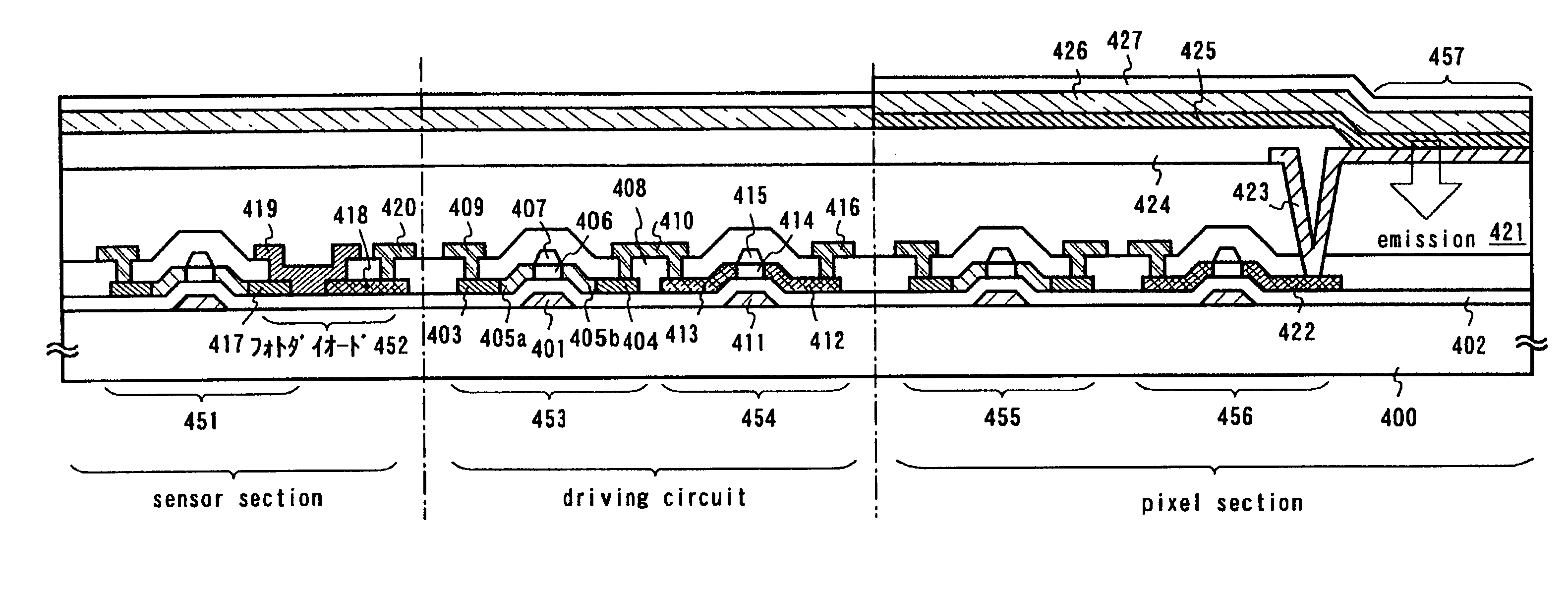
[0054]In the present embodiment, a cross-sectional structure (in a state before sealing) included in a light emitting module in accordance with the present invention will be described. In the present embodiment, there will be described an example of a light emitting device (in a state before sealing) which has a sensor section, a pixel section, and a driving circuit for driving the pixel section on the same insulating body. Here, the sensor section shows a reset TFT and a photodiode connected to the reset TFT, and the driving circuit shows a CMOS circuit which is a basic unit, and the pixel section shows one pixel.

[0055]In FIG. 4, a reference numeral 400 is an insulting body (made of an insulating substrate, an insulating film, or a substrate with an insulating film on the surface) on which a sensor section, a driving circuit, and a pixel section are formed. The sensor section is provided with a reset TFT 451 and a photodiode 452. Also, the driving circuit...

embodiment 2

(Embodiment 2)

[0079]In the present embodiment, there will be described an example of a light emitting device (however, in the state before sealing) with a structure different from the embodiment 1. Here, in the present embodiment, description will be made in the different parts from the embodiment 1. The description of the embodiment 1 may be referred to on parts with the same reference symbols as the parts in FIG. 4.

[0080]In FIG. 6, a sensor section, a driving circuit, and a pixel section are formed on an insulating body 400. The sensor section includes a reset TFT 451 and a photodiode (photo-sensor) 601, and the driving circuit includes a CMOS circuit comprising an n-channel type TFT 453 and a p-channel type TFT 454, and the pixel section includes a switching TFT 455, a current control TFT 456, and an EL element 457.

[0081]The present embodiment is different from the embodiment 1 in the structure of the photodiode 601. The photodiode is formed of a wiring 603 which is to be the sou...

embodiment 3

(Embodiment 3)

[0084]In the present embodiment, there will be described an example of a light emitting device (however, in the state before sealing) with a different structure from the embodiment 1. Here, in the present embodiment, description will be made in the different parts from the embodiment 1. The description of the embodiment 1 may be referred to on parts with the same reference symbols as the parts in FIG. 4.

[0085]In FIG. 7, a sensor section, a driving circuit, and a pixel section are formed on an insulating body 400. The sensor section includes a reset TFT 701 and a photodiode (photo-sensor) 702, and the driving circuit includes a CMOS circuit comprising an n-channel type TFT 703 and a p-channel type TFT 704, and the pixel section includes a switching TFT 705, a current control TFT 706, and an EL element 457.

[0086]First, the present embodiment is characterized in that the source line or the drain line of each TFTs is formed so as to cover a channel region. The structure of...


PUM


Abstract

The object of the present invention is to provide a light emitting module which is excellent in visibility and can reduce power consumption.The light emitting module includes a light emitting device containing at least a pixel section 101 and a sensor section 104, which are formed on the same insulating body, and further includes means for sensing illuminance of a use environment with the sensor section 104 and for adjusting luminance of a light emitting element according to the illuminance to keep a ratio of the luminance to the illuminance of the use environment at a constant value.

Description

BACKGROUND OF THE INVENTION[0001]1. Field of the Invention[0002]The present invention relates to a module (hereinafter referred to as a light emitting module) including a device (hereinafter referred to as a light emitting device) comprising an element sandwiching a light emitting material (hereinafter referred to as a light emitting element) between electrodes. In particular, the present invention relates to a light emitting module comprising a light emitting element (hereinafter referred to as an EL element) using a compound producing EL (Electro Luminescence) as the light emitting material. Here, an organic EL display and an organic light emitting diode (hereinafter referred to as an OLED) is included in the light emitting device in accordance with the present invention.[0003]Further, the light emitting material used in the present invention includes all materials emitting light (phosphorescence and / or fluorescence) through singlet excitation, triplet excitation or both of them.[...

Claims


Application Information

Patent Timeline
Patent Type & Authority Patents(United States)
IPC IPC(8): G09G3/30G09G3/20H05B44/00G09G3/32H01L21/77H01L21/84H01L25/16H01L27/12H01L27/32H01L51/50H01L51/52H05B33/14
CPCG01J1/44G09G3/3275H01L25/167H01L27/3269H01L51/5281H01L2924/0002G09G2300/0842G09G2300/0852G09G2310/0251G09G2320/0233G09G2320/0285G09G2320/029G09G2320/043G09G2320/0626G09G2330/021G09G2360/144G09G2360/18H01L27/12H01L27/1214H01L2924/00H01L27/1288H01L27/124H10K59/13G01J1/4204H10K59/8791G09G3/30H10K50/86
Inventor YAMAZAKI, SHUNPEIKOYAMA, JUN
Owner SEMICON ENERGY LAB CO LTD
Why Eureka
Try Eureka