Method of producing biaxially textured buffer layers and related articles, devices and systems

a buffer layer and biaxial texture technology, applied in the direction of superconducting magnets/coils, magnetic bodies, natural mineral layered products, etc., can solve the problems of slow process, high cost, speed and price of such process, and difficult to employ large-scale production methods

Inactive Publication Date: 2006-07-04
SUPERPOWER INC
View PDF15 Cites 14 Cited by
  • Summary
  • Abstract
  • Description
  • Claims
  • Application Information

AI Technical Summary

Problems solved by technology

While the above-described IBAD process has provided the desired biaxial texture requiring a relatively high thickness (>1 μm), such as by use of a YSZ film deposited in the presence of the Ar+beam, the process is relatively slow and as a result expensive.
The speed and price of such process is a significant issue in the large-scale production of superconducting tapes since it would affect the ability to produce a low-cost HTS tape.
This approach is difficult to employ for large-scale production.
Also, the quality of MgO films deposited by IBAD has been found to be extremely sensitive to minor variations in the processes and structures used for this material.

Method used


Image

  • Method of producing biaxially textured buffer layers and related articles, devices and systems
  • Method of producing biaxially textured buffer layers and related articles, devices and systems
  • Method of producing biaxially textured buffer layers and related articles, devices and systems

Examples


example 1

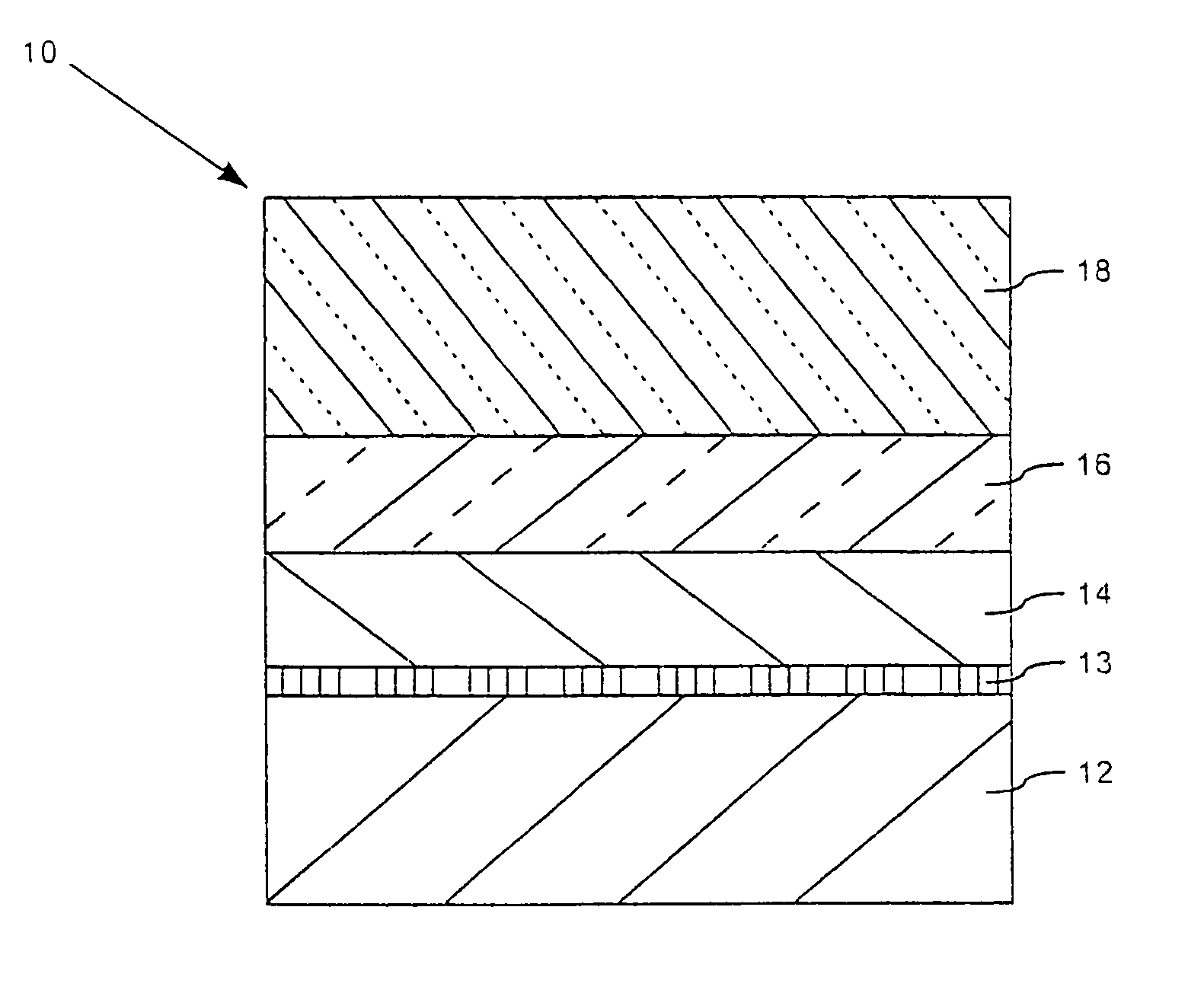
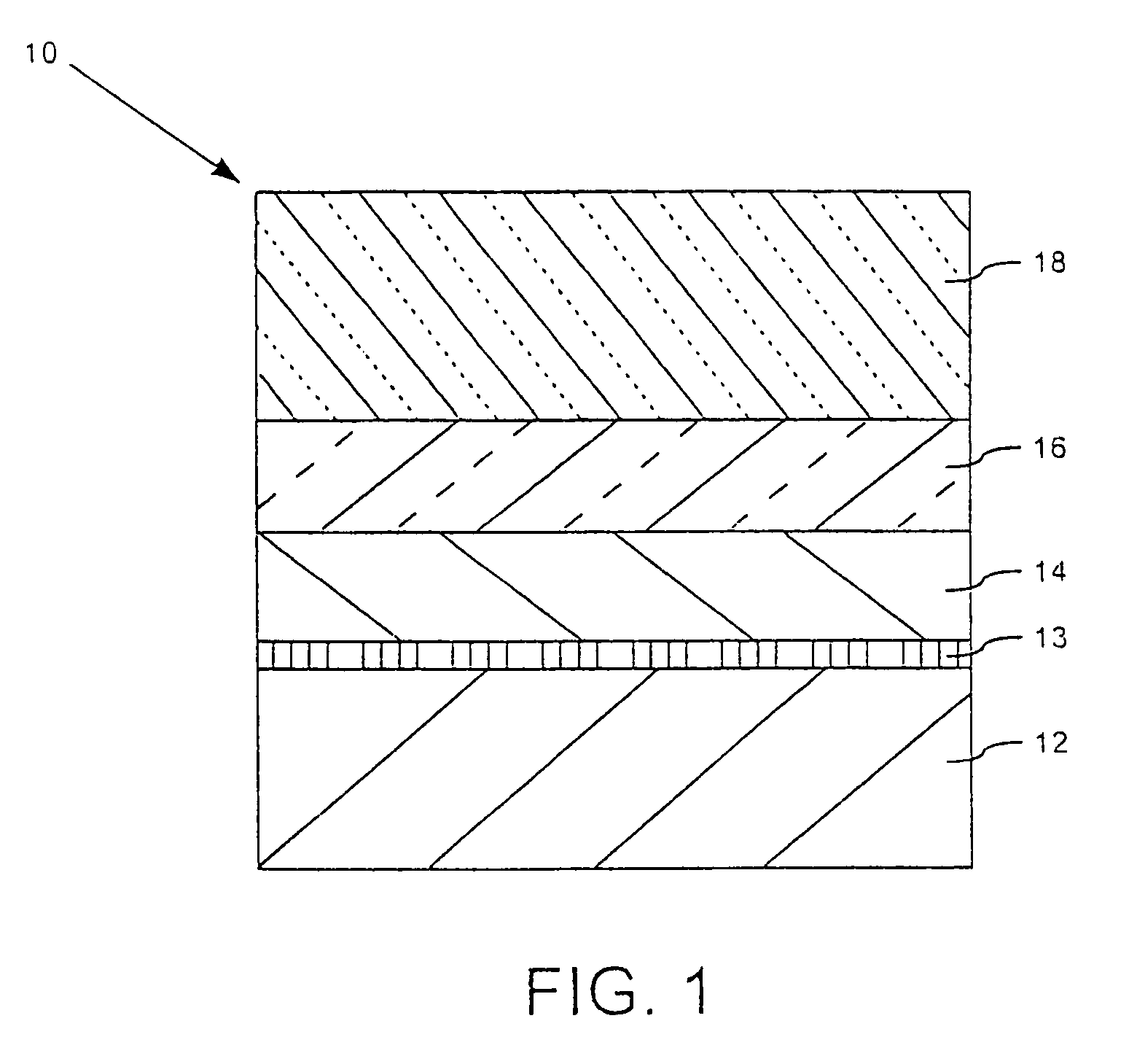
[0053]A Ni-based alloy substrate is provided for film growth. The substrate is cleaned with solvents, such as acetone, methanol, and trichloroethylene. The substrate is mounted in a pulsed-laser deposition chamber for thin film deposition. A polycrystalline yttria-stabilized zirconia (YSZ) protective layer is deposited on the substrate using pulsed laser deposition at about 25.degree. C. under vacuum. This protective layer prevents chemical reactions between layer 1 and the substrate.

[0054]The coated substrate is heated to about 700.degree. C. in vacuum for the deposition of an YBa2Cu3O7 thin film (Layer 1). A YBa2Cu3O7 film of thickness about 300 nm is deposited at about 700.degree. C. in about 200 mTorr of oxygen. The film is c-axis oriented, but randomly oriented in-plane. The substrate is then transferred to a thin-film deposition system equipped with an ion gun. The substrate is heated to a temperature suitable for the epitaxial growth of MgO on YBa2Cu3O7 on Layer 1. Pulsed las...

example 2

[0055]A Ni-based alloy substrate is provided for film growth. The substrate is cleaned with solvents, such as acetone, methanol, and trichloroethylene. The substrate is mounted in a pulsed-laser deposition chamber for thin film deposition. A MgO film of thickness of about 100 nm (Layer 1) is deposited at about 25.degree. C. in vacuum. The MgO layer will be (001) textured. The coated substrate is then transferred to a thin-film deposition system equipped with an ion gun. A second layer of MgO (Layer 2) is grown in the presence of an Ar ion beam, the ion beam being directed along either the [111] or [110] crystallographic direction of MgO. The second MgO layer (Layer 2) will be biaxially textured.


PUM

PropertyMeasurementUnit
crystallite sizeaaaaaaaaaa

Abstract

A superconductor article includes a substrate and a first buffer film disposed on the substrate. The first buffer film includes a polycrystalline material. An IBAD (ion-beam assisted deposition) second buffer film is disposed on the first buffer film, the second buffer film having a biaxial crystal texture. A superconductor layer can be disposed on the second buffer film.

Description

CROSS-REFERENCE TO RELATED APPLICATION(S)[0001]The present application is a continuation-in-part and claims priority from U.S. Utility patent application Ser. No. 10 / 457,184, filed Jun. 9, 2003 now U.S. Pat. No. 6,849,580, entitled “METHOD OF PRODUCING BIAXIALLY TEXTURED BUFFER LAYERS AND RELATED ARTICLES, DEVICES AND SYSTEMS,” naming inventors David P. Norton and Venkat Selvamanickam, which application is incorporated by reference herein in its entirety.FIELD OF THE INVENTION[0002]The invention relates to biaxially textured buffer layers and articles, devices and systems made therefrom, including superconductor wires and tapes.BACKGROUND OF THE INVENTION[0003]Much of the effort to develop a high temperature superconducting (HTS) wire or tape has focused on coated conductors based on the epitaxial growth of high temperature superconducting (HTS) films on tapes that possess a biaxially-textured surface. Superconducting films with critical current densities in excess of 1 MA / cm2 at 77...

Claims


Application Information

Patent Timeline
Patent Type & Authority Patents(United States)
IPC IPC(8): H01B12/00H01F6/00H01L39/00C30B25/18C30B29/22H01L39/24
CPCC30B25/18H01L39/2461C30B29/22Y10S428/93H10N60/0632Y02E40/60H01B12/02
Inventor SELVAMANICKAM, VENKAT
Owner SUPERPOWER INC
Why Eureka
Try Eureka