Induction sensor using printed circuit

a printed circuit and induction sensor technology, applied in the field of induction sensors, can solve the problems of high probability of bill jamming, high cost of coils and other elements of this type of induction sensor manufacturing, and complex electronic circuitry or individual adjustment elements are often required, so as to improve the dependence of sensors signal and improve the effect of signal dependen

Inactive Publication Date: 2006-07-04
CRANE CANADA
View PDF9 Cites 14 Cited by
  • Summary
  • Abstract
  • Description
  • Claims
  • Application Information

AI Technical Summary

Benefits of technology

[0010]According to another aspect, a method of improving of the dependence of the sensors signal verses the distance between the sensor and the document includes the arrangement of two planar induction sensors with individual associated electronic circuits placed on the opposite sides of the validator channel. An analysis of the signal from one sensor allows calculating correction coefficients for multiplication the signal from second sensor. It improves the dependence of signal on the distance between the second sensor and the tested document.
[0011]Various implementations include one ore more of the following features. The planar induction sensor could comprise several current transformers, each being connected to its own operating coil. The planar induction sensor could comprise several current transformers, connected to common operating coil. The primary coil of current transformer may contain two spiral coils, placed in two nearest to opposi...

Problems solved by technology

Due to this dispersion complicated electronic circuitry or individual adjusting elements are often required.
Such coils and other elements of this type of induction sensors are expensive to manufacture.
Such an arrangement leads to a high p...

Method used


Image

  • Induction sensor using printed circuit
  • Induction sensor using printed circuit
  • Induction sensor using printed circuit

Examples


Embodiment Construction

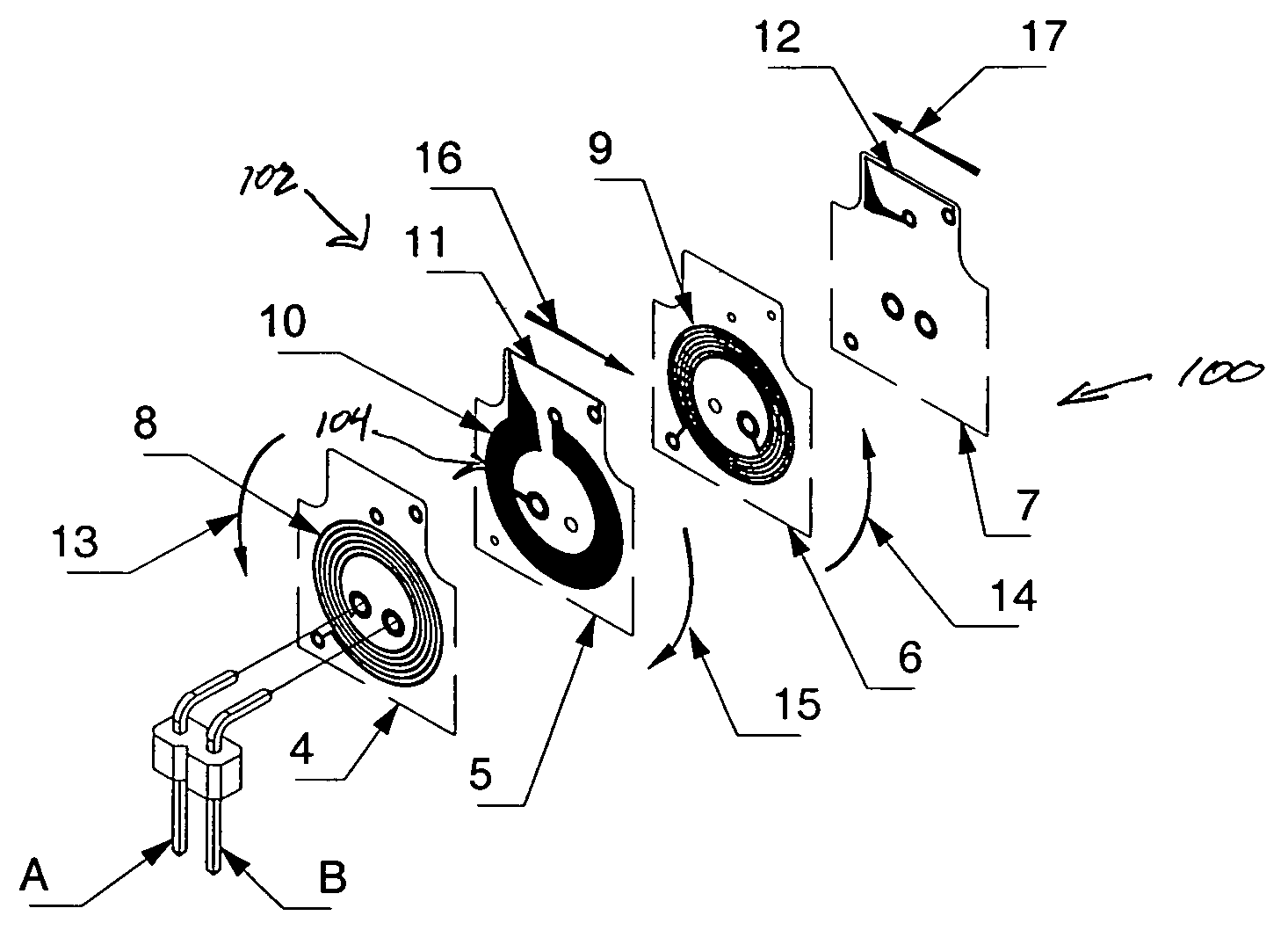
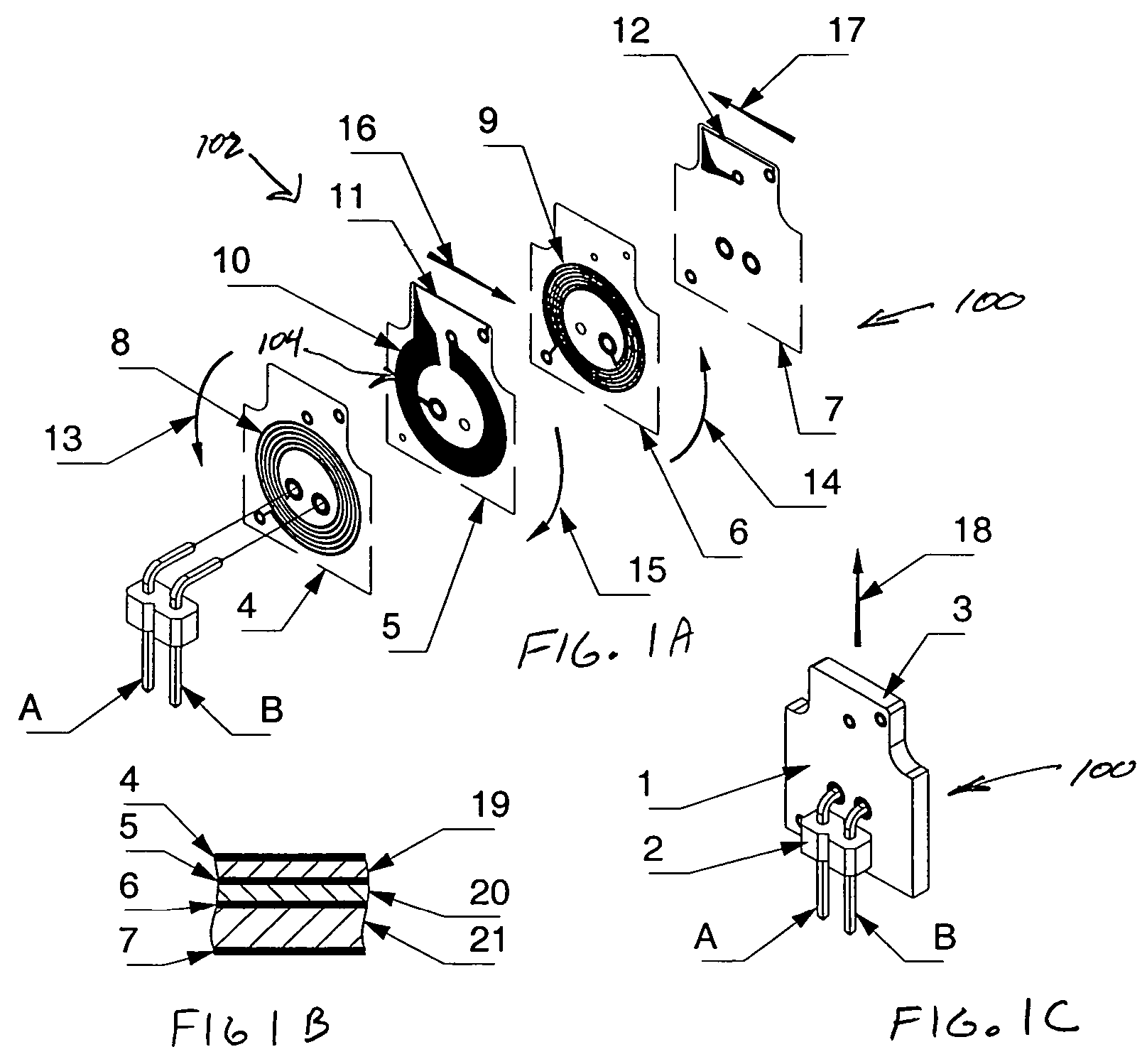
[0030]The planar induction sensor 100 shown on FIG. 1 comprises multilayer printed board 1 and two-wire connector 2. This sensor has active zone situated near edge 3 of the multilayer printed board 1. The multilayer printed board 1 comprises four active layers 4, 5, 6 and 7, said active layers are separated by glass fibre laminat separation dielectric layers 19, 20 and 21. All holes, shown on FIGS. 1A, 1B and 1C have inner metallization allowing connection between the wires in active layers 4, 5, 6 and 7 associated with the corresponding hole.

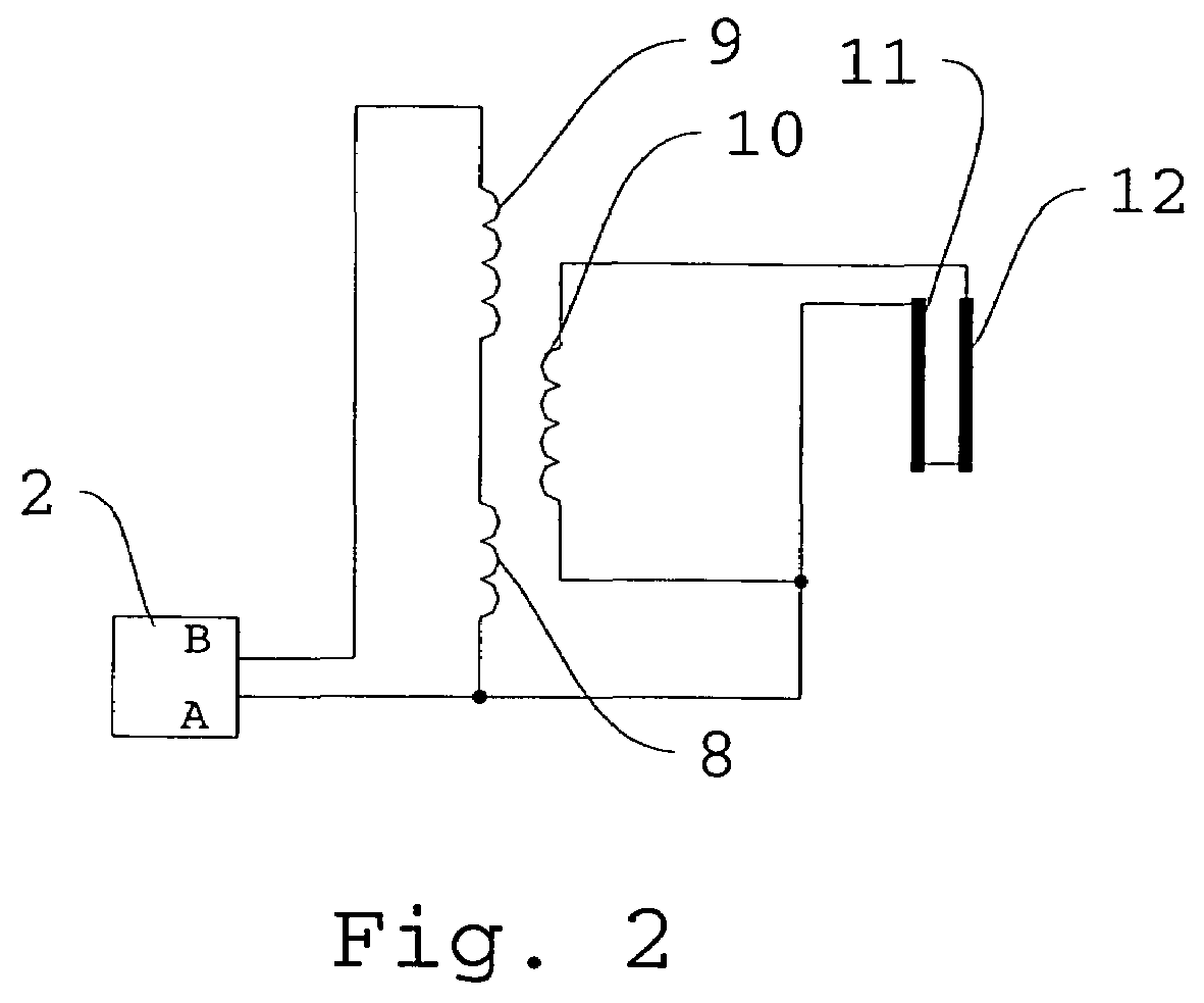
[0031]In active layers 4, 5 and 6 there is situated a current transformer 102 being formed by two series primary spiral-type coils 8 and 9 and a secondary one-turn coil 10. Secondary coil 10 of current transformer is connected to the operating coil 104 being formed by two wires 11 and 12. Wires 11 and 12 of the operating coil are situated in the nearest vicinity to sensing edge 3 of multilayer printed board 1.

[0032]Instant directions of alterna...


PUM


Abstract

A planar induction sensor for sensing of security features of documents having changing magnetic and (or) conducting properties is of a multilayer printed circuit board design. The sensor comprises a planar current transformer with a spiral-type primary coils and one or several turns of secondary coil in an adjacent layer of the printed circuit board. The secondary coil of the current transformer is connected to an operating coil, which is situated at a sensing edge of the sensor. The operating coil can be formed by external wires or can be incorporated in the circuit board of the current transformer. When a security element, made from the magnetic or conductive material moves past the sensing edge of the sensor, a change in inductance of the induction sensor occurs. In a preferred embodiment, two induction sensors with individual associated electronic circuits were located on opposite sides of validator channel. Analysis of both signals from the sensors allows correction of the signal to reduce variation caused by changing distance of the security document from each sensor.

Description

FIELD OF THE INVENTION[0001]The present invention is directed to an induction sensor for detection of magnetic and conductivity elements passed in proximity to the active part of a planar induction sensor. The planar induction sensor has particular application in verification devices for verifying the authenticity of documents, such as banknotes, that have magnetic or conductive security elements.BACKGROUND OF THE INVENTION[0002]Many security documents, such as bank notes, include different security elements including security dyes, security inks and security threads. These security elements typically have magnetic and (or) conducting properties which can be detected. Counterfeited documents sometimes have magnetic properties in those regions, where an authentic document has not any magnetic properties and therefore detection of these elements and the location is useful to determine whether a banknote is authentic.[0003]There are various types of induction sensors, which are able to...

Claims


Application Information

Patent Timeline
IPC IPC(8): G01N27/82G07D7/04H01F27/28
CPCG01D5/204G07D7/04H01F17/0013H01F19/08H01F2017/0073H01F21/06H01F27/2804
Inventor SALTSOV, LEONBARCHUK, VOLODYMYRANDROSYUK, SERGIYBAYDIN, DMITROGRZHIBOVSKYY, VITALIYYAVORSKYY, YEVGENIYGAPONYUK, GENNADIY
Owner CRANE CANADA
Why Eureka
Try Eureka