Fractional-Bit Systems

a technology of fractional-bit storage and data storage, applied in the field of electronic systems, can solve the problems of inefficient approach and impracticality of incrementing b by 1 between product generations, and achieve the effect of optimizing the storage density of fractional-bit storage systems, improving transmission bandwidth of transmission systems, and improving storage density of storage systems

Inactive Publication Date: 2006-07-04
ZHANG GUOBIAO
View PDF9 Cites 95 Cited by
  • Summary
  • Abstract
  • Description
  • Claims
  • Application Information

AI Technical Summary

Problems solved by technology

It has been realized that the conventional approach of incrementing b by 1 between product generations has become impractical.
However, this approach is inefficient for a fractional-bit system (FIG. 4).

Method used


Image

  • Fractional-Bit Systems
  • Fractional-Bit Systems
  • Fractional-Bit Systems

Examples


Embodiment Construction

[0034]Those of ordinary skills in the art will realize that the following description of the present invention is illustrative only and is not intended to be in any way limiting. Other embodiments of the invention will readily suggest themselves to such skilled persons from an examination of the within disclosure.

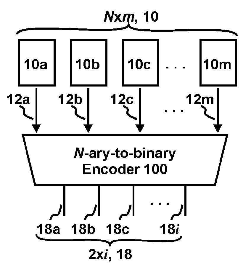
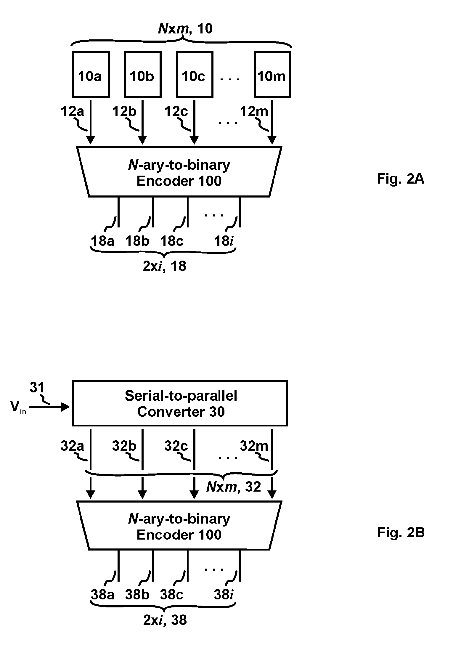
[0035]FIG. 2A illustrates a basic N-ary fractional-bit parallel-input system. In a parallel-input system, a plurality of cells are accessed in parallel. Typical parallel-input system is semiconductor memory (e.g. flash, EPROM, EEPROM, MRAM, FeRAM, DRAM, SRAM, variable-resistance memory such as phase-change memory or Ovonyx unified memory (OUM), mask-programmable memory, diode memory, antifuse memory, etc.) Semiconductor memory is array-based and easy to provide parallel access. The N-ary fractional-bit parallel-input system in FIG. 2A is comprised of a word 10 and an N-ary-to-binary encoder 100. The word 10 comprises m N-ary cells 10a, 10b . . . 10m, with each cell having N...


PUM


Abstract

The present invention abandons the conventional approach of incrementing bits-per-cell b by 1, but allows increments of states-per-cell N by as little as 1 between product generations. Because N is no longer an integral power of 2, b takes a fractional value, resulting in a fractional-bit system. In a fractional-bit system, cells are decoded in unit of word. By adjusting the word-width, the system efficiency can be optimized.

Description

CROSS-REFERENCE TO RELATED APPLICATIONS[0001]This application relates to a first provisional application Ser. No. 60 / 559,683, Filed Apr. 4, 2004 and a second provisional application Ser. No. 60 / 594,141, Filed Mar. 14, 2005.SYMBOLS USED IN THE SPECIFICATION[0002]N—states-per-cell, i.e. number of possible states per cell, a positive integer;[0003]m—word-width, i.e. number of cells in a word, a positive integer;[0004]n—the maximum number of binary bits that can be represented by m N-ary cells, a positive integer;[0005]b—bits-per-cell, i.e. average number of bits represented by each cell, could be a non-integer;[0006]β—efficiency of N-ary fractional-bit system.BACKGROUND[0007]1. Technical Field of the Invention[0008]The present invention relates to the field of electronic systems, more particularly to data storage and transmission systems.[0009]2. Prior Arts[0010]Multi-level memory cell can be used to improve the storage density. A multi-level cell (e.g. an N-level flash cell) can store...

Claims


Application Information

Patent Timeline
Patent Type & Authority Patents(United States)
IPC IPC(8): H03M5/02H03M7/16H03M7/34
CPCH03M7/165G11C11/56G11C8/10G11C7/1006
Inventor ZHANG, GUOBIAO
Owner ZHANG GUOBIAO
Why Eureka
Try Eureka