

Stability metrics for placement to quantify the stability of placement algorithms
a placement algorithm and stability measurement technology, applied in the field of fabrication and design of semiconductor chips and integrated circuits, can solve the problems of large number of cells, difficult computer-aided design, and complicated connections between cells,
- Summary
- Abstract
- Description
- Claims
- Application Information
AI Technical Summary
Benefits of technology
Problems solved by technology
Method used
Image

Examples
Embodiment Construction
)
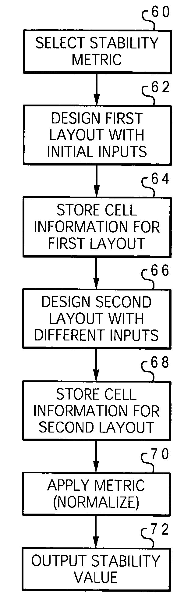
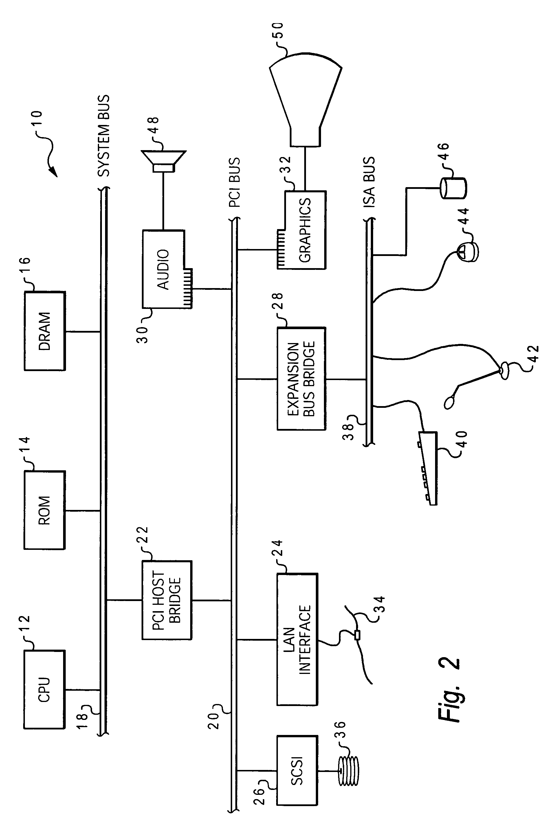
[0026]The present invention provides a method for assessing the stability of computer-aided design (CAD) tools used in mapping the physical layout (placement) and wiring (routing) of logic cells for the design of an integrated circuit chip. The invention quantifies the stability of these tools using numeric computations, as explained further below, which are carried out on a data processing system or computer. FIG. 2 depicts one embodiment 10 of a computer system programmed to carry out evaluation of an industrial placement tool in accordance with one implementation of the present invention. System 10 includes a central processing unit (CPU) 12 which carries out program instructions, firmware or read-only memory (ROM) 14 which stores the system's basic input / output logic, and a dynamic random access memory (DRAM) 16 which temporarily stores program instructions and operand data used by CPU 12. CPU 12, ROM 14 and DRAM 16 are all connected to a system bus 18. There may be additional ...
PUM
 Abstract
Description
Claims
Application Information