

A Data Transmission Link Fault Monitoring Technology Based on AC-Coupled LVDS Standard
An AC coupling and data transmission technology, applied in the direction of the fault location, etc., can solve the problems of increased jitter, difficult generation of comparison reference voltage, poor matching between short-connected resistance and on-chip resistance, etc., to prevent power supply noise and avoid judgment noise, comparison reliable results
- Summary
- Abstract
- Description
- Claims
- Application Information
AI Technical Summary
Problems solved by technology
Method used
Image

Examples
Embodiment 1
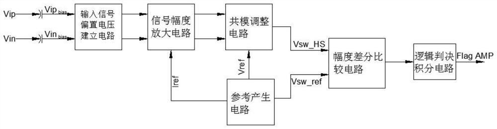
[0044] Such as figure 1 and Figure 5 As shown, the present invention provides a data transmission link fault monitoring technology based on the AC-coupled LVDS standard, including an input signal bias voltage establishment circuit (Input Bias Setting Circuits), a signal amplitude amplification circuit (HS AMP Regulator), a reference Generation circuit (Reference Generator), common mode adjustment circuit (HSCM Conditioner), amplitude differential comparison circuit (Diff Comparator) and logic decision integration circuit (Slicer), the input signal bias voltage establishment circuit establishes a suitable for the AC-coupled input data signal The DC bias working voltage, and then transmit the input data signal to the signal amplitude amplifier circuit to amplify with the rated voltage gain, the signal amplitude amplifier circuit further transmits the amplified input data signal to the common-mode adjustment circuit, and the common-mode adjustment circuit After adjusting the co...
Embodiment 2
[0048] In order to realize the above scheme, three key indicators should be guaranteed during circuit design: one is the consistency of the input signal gain; the other is the common-mode matching of the input signals at both ends of the comparator; the third is the accuracy of the signal amplitude threshold voltage; Specific instructions are given in the circuit architecture analysis and performance index design;
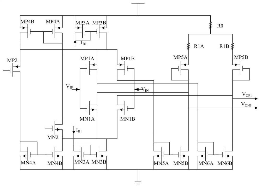
[0049] In the LVDS standard, it is defined that the common-mode range of the input signal is 0.05V-2.4V; in order to avoid the influence of the change of the input common-mode voltage on the gain, the present invention adopts a rail-to-rail constant transconductance amplifier structure, circuit principle Figure such as figure 2 As shown, V IP / V IN is the LVDS differential input signal, V OP1 / V ON1 It is the differential output signal of the amplifier; the complementary amplifier stage is composed of MN1A / MN1B and MP1A / MP1B, combined with the common-mode volt...
PUM
 Abstract
Description
Claims
Application Information