Method for separating sapphire wafer into chips

a sapphire wafer and chip technology, applied in the field of sapphire wafer separation, can solve the problems of difficult to precisely scribe the sapphire wafer the surface of the polished sapphire wafer is not easily scribed using the diamond tip, and the inability to substantially display the total natural colors, etc., to achieve the effect of preventing the defect of the shape of the obtained chips, reducing the quantity of abrasion of the expansive diamond tip, and easy-

Inactive Publication Date: 2006-07-11
SAMSUNG ELECTRONICS CO LTD
View PDF8 Cites 19 Cited by
  • Summary
  • Abstract
  • Description
  • Claims
  • Application Information

AI Technical Summary

Benefits of technology

[0011]Therefore, the present invention has been made in view of the above problems, and it is an object of the present invention to provide a method for separating a sapphire wafer serving as a substrate, provided with semiconductor elements such as LEDs formed thereon, into chips, in which the sapphire wafer is easily and efficiently scribed by controlling stress on the rear surface of the sapphire wafer, thus preventing defects in the shape of the obtained chips and reducing the quantity of abrasion of an expansive diamond tip.

Problems solved by technology

However, the yellowish green LED emits a beam having a brightness lower than those of the red and blue LEDs and a wavelength of 565 nm, which is unnecessary for displaying the three primary colors of light.
Accordingly, with the yellowish green LED, it is impossible to substantially display the total natural colors.
In the above-described conventional method for separating the sapphire wafer into the chips, since the polished sapphire wafer has a low surface roughness (Ra) and a low stress, the surface of the polished sapphire wafer is not easily scribed using the diamond tip.
That is, since the diamond tip skids on the surface of the sapphire wafer, it is difficult to precisely scribe the sapphire wafer using the diamond tip.
The difficulty in precisely scribing the sapphire wafer using the diamond tip causes cracks on chips separated from the sapphire wafer as shown in FIGS. 4a and 4b, thus generating defects in the shape of the chips and reducing yield of the chips.
Particularly, the conventional method for separating the sapphire wafer into the chips increases the quantity of abrasion of the expensive diamond tip, thus reducing productivity in manufacturing the chips and increasing unit cost of obtained chip products.

Method used


Image

  • Method for separating sapphire wafer into chips
  • Method for separating sapphire wafer into chips
  • Method for separating sapphire wafer into chips

Examples


Embodiment Construction

[0021]Now, preferred embodiments of the present invention will be described in detail with reference to the annexed drawings.

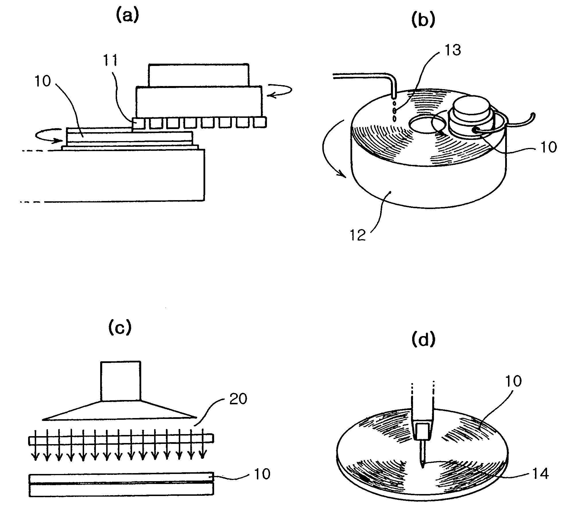
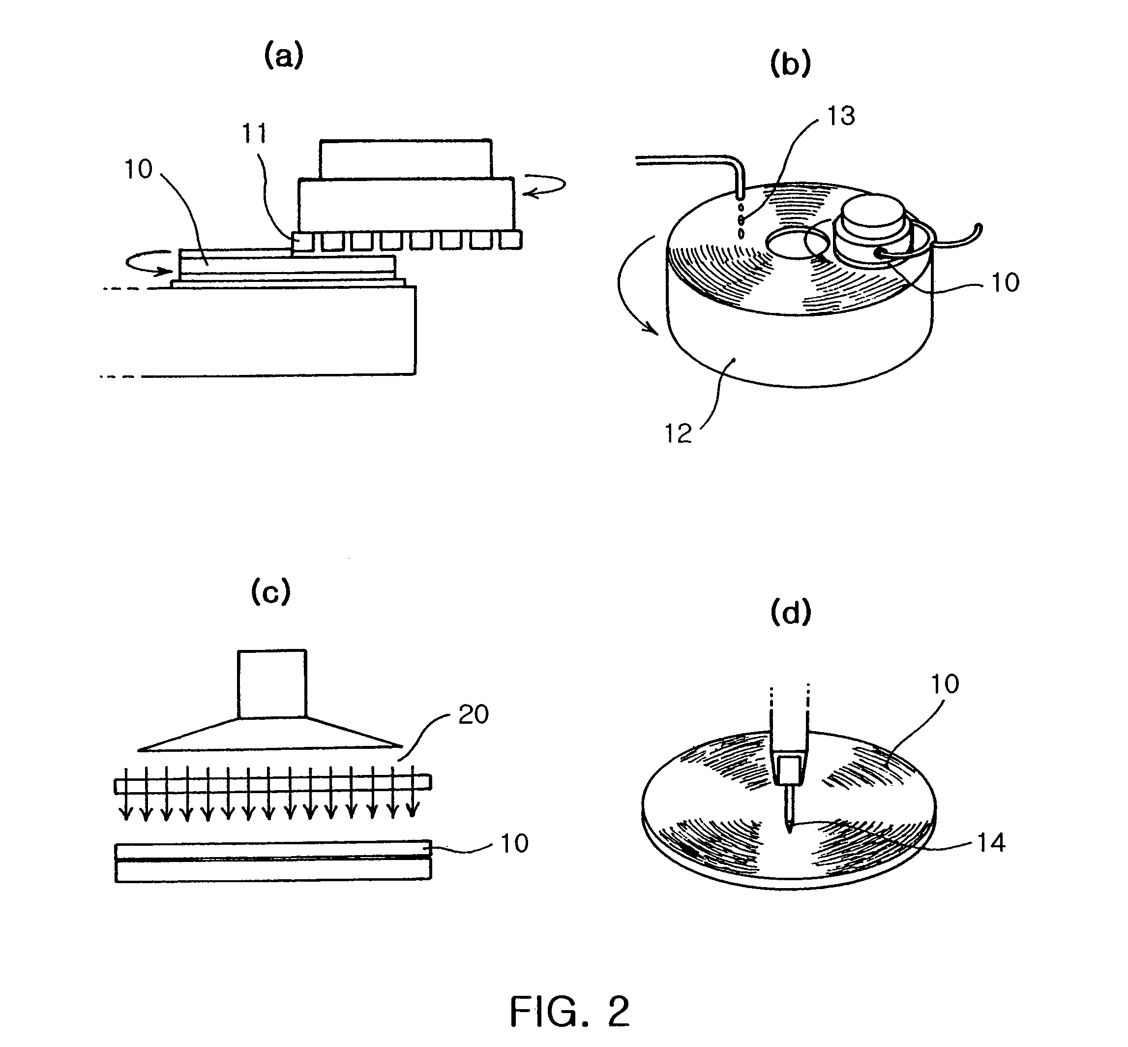
[0022]FIGS. 2a to 2d are schematic views illustrating a method for separating a sapphire wafer 10 into chips in accordance with the present invention. As shown in FIG. 2a, a rear surface of the sapphire wafer 10 is ground using a rotating diamond wheel 11 so that the sapphire wafer 10 has a designated thickness (for example, 115 μm).

[0023]As shown in FIG. 2b, the ground sapphire wafer 10 is lapped and polished. In the lapping step, the ground sapphire wafer 10 is mounted on a lapping plate 12, and then ground using a diamond slurry 13 having a particle size of 6 μm so that the sapphire wafer 10 has a designated thickness (for example, 8 μm). After the lapping step, the sapphire wafer 10 is polished using a diamond slurry 13 having a particle size of 3 μm smaller than the particle size of the diamond slurry 13 used in the lapping step in the same manner as the ...


PUM

PropertyMeasurementUnit
heightaaaaaaaaaa
thicknessaaaaaaaaaa
surface roughnessaaaaaaaaaa

Abstract

Disclosed is a method for efficiently separating a sapphire wafer serving as a substrate, on which semiconductor elements are formed, into unit chips by scribing the sapphire wafer, after grinding and lapping a rear surface of the sapphire wafer and then sand-blasting the sapphire wafer. The method includes the steps of: (a) grinding a rear surface of the sapphire wafer so that the sapphire wafer has a designated thickness; (b) lapping the rear surface of the ground sapphire wafer so that the sapphire wafer has a designated thickness; (c) polishing the rear surface of the lapped sapphire wafer so that the sapphire wafer has a designated thickness; (d) sand-blasting the rear surface of the polished sapphire wafer by uniformly blasting particles at a designated pressure during a designated time onto the rear surface of the polished sapphire wafer; and (e) scribing the rear surface of the sand-blast ground sapphire wafer.

Description

BACKGROUND OF THE INVENTION[0001]1. Field of the Invention[0002]The present invention relates to a method for separating a sapphire wafer, adapted to manufacture a GaN semiconductor light emitting diode (LED), into chips, and more particularly to a method for separating a sapphire wafer into chips by scribing the sapphire wafer, after grinding, lapping and polishing a rear surface of the sapphire wafer and then sand-blasting the sapphire wafer, thus allowing the sapphire wafer to be efficiently scribed.[0003]2. Description of the Related Art[0004]Recently, LED displays, serving as visual information transmission media, starting from providing alpha-numerical data have been developed to provide various moving pictures such as CF images, graphics, video images, etc. Further, the LED displays have been developed so that light emitted from the displays is changed from a solid color into colors in a limited range using red and yellowish green LEDs and then into total natural colors using...

Claims


Application Information

Patent Timeline
Patent Type & Authority Patents(United States)
IPC IPC(8): H01L21/48G03C5/00H01L21/78H01L29/22H01L33/00
CPCH01L33/0095H01L21/78
Inventor YOON, JEONG GOOOH, BANG WONYI, KUK HWEA
Owner SAMSUNG ELECTRONICS CO LTD
Why Eureka
Try Eureka