

Tandem OLEDs having low drive voltage
a technology of drive voltage and tandem oled, which is applied in the direction of discharge tube/lamp details, discharge tube luminescnet screens, organic semiconductor devices, etc., can solve the problems of not revealing a tandem oled containing more than two el units and a drive voltage suitable for the common tft drive circuitry, and achieves low voltage drop, low drive voltage, and high luminous efficiency
- Summary
- Abstract
- Description
- Claims
- Application Information
AI Technical Summary
Benefits of technology
Problems solved by technology
Method used
Image

Examples
example 5
[0172]A low voltage OLED was constructed with the similar fabrication methods to those used in Example 1, and the deposited layer structure is:
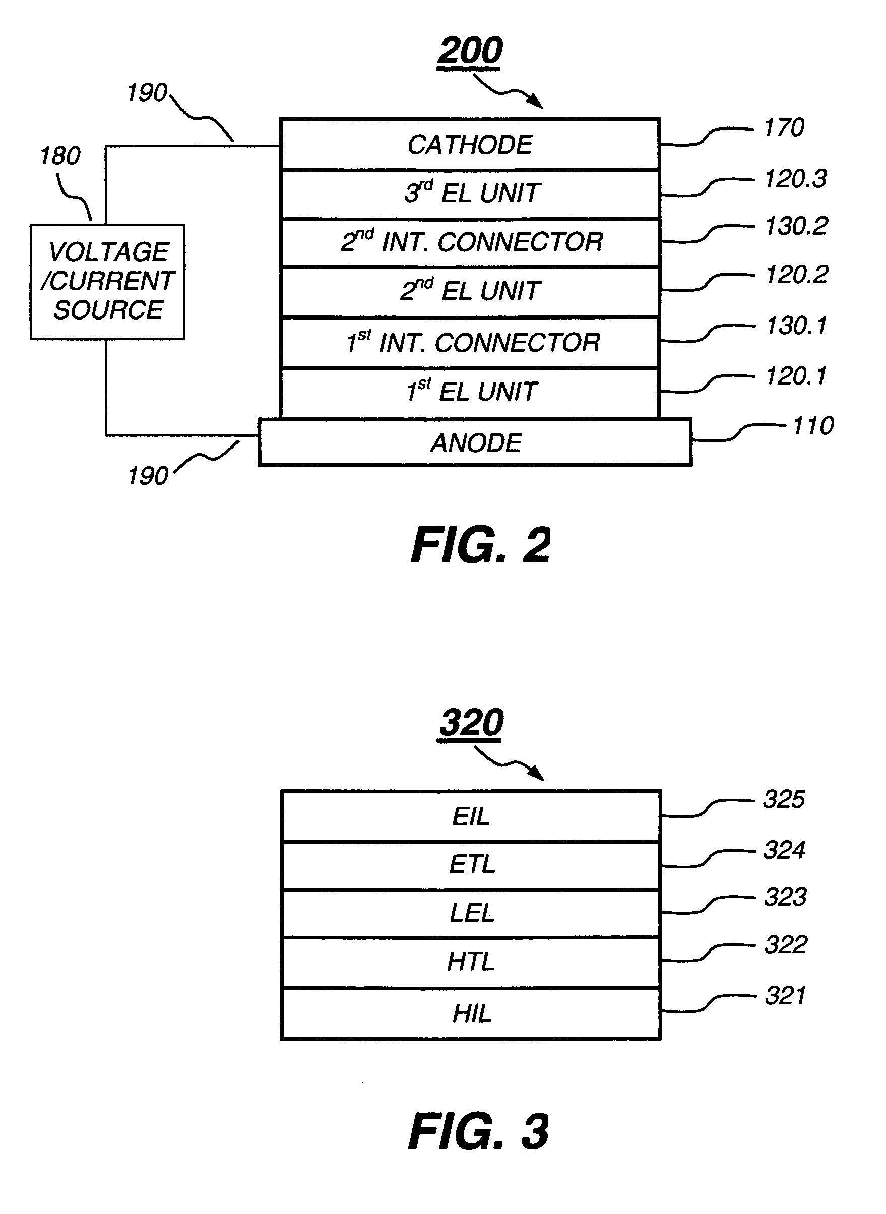
1. EL Unit:
[0173]a) an HIL, 70 nm thick, including m-TDATA doped with 4 vol % F4-TCNQ;
[0174]b) an HTL, 5 nm thick, including NPB;
[0175]c) a LEL, 12 nm thick, including Alq doped with 1.0 vol % C545T;
[0176]d) an ETL, 5 nm thick, including 4,7-diphenyl-1,10-phenanthroline (Bphen); and
[0177]e) an EIL, 40 nm thick, including Bphen doped with about 1.5 vol % lithium.
2. Cathode: approximately 210 nm thick, including MgAg (formed by coevaporation of about 95 vol. % Mg and 5 vol. % Ag).
[0178]This OLED requires a drive voltage of about 3.8 V to pass 20 mA / cm2. Under this test condition, the device has a luminance of 2298 cd / m2, and a luminous efficiency of about 11.5 cd / A. Its CIEx and CIEy are 0.289, 0.649, respectively, with an emission peak at 521 nm. Moreover, the drive voltage is about 3.5 V under the test condition of 1000 cd / m2. The EL performa...
example 6
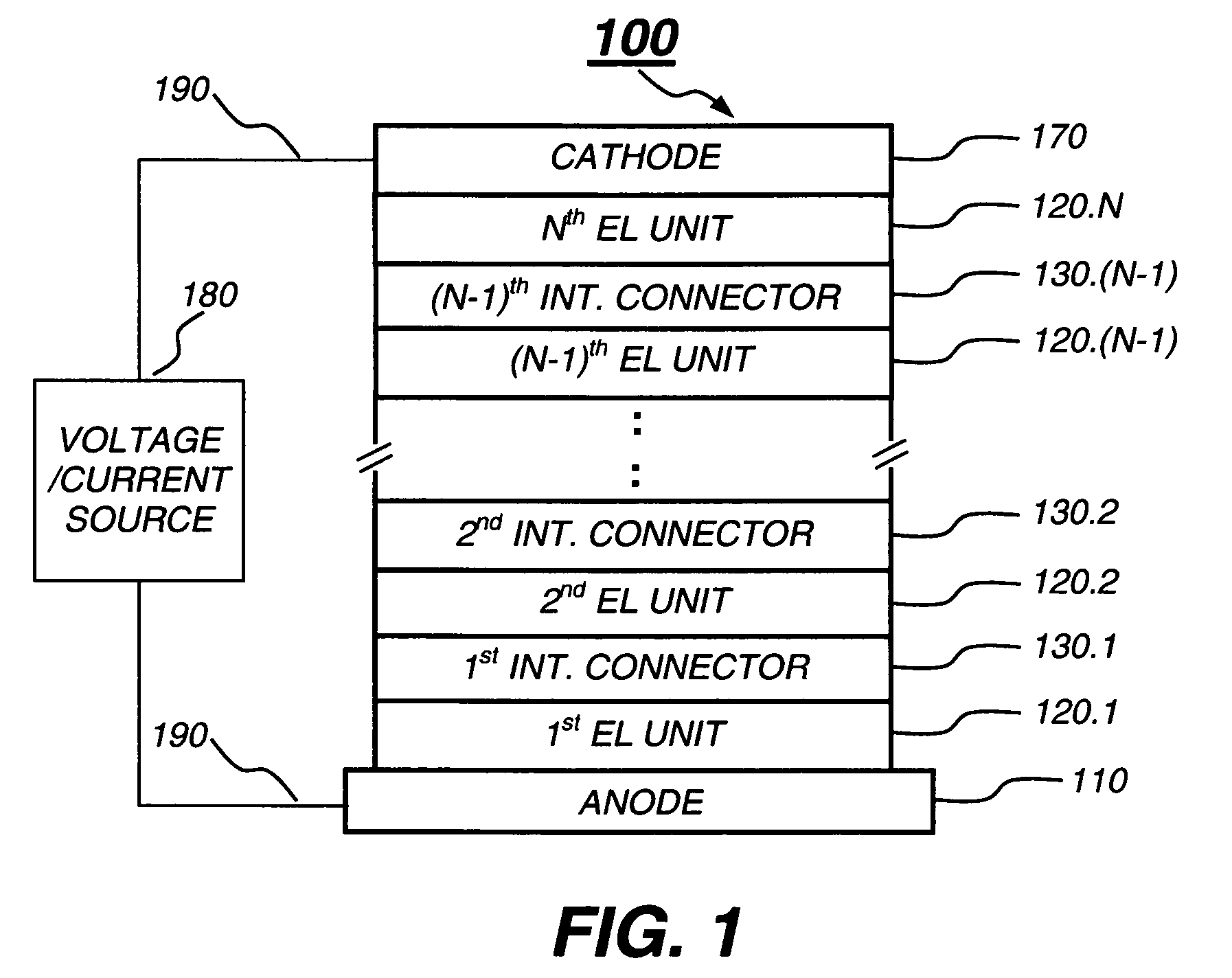
[0179]A tandem OLED according to the present invention was constructed with the similar fabrication methods to those used in Example 1, and the deposited layer structure is:
1. 1st EL Unit:
[0180]The 1st EL unit is the same as the EL unit in Example 5.
2. 1st Intermediate Connector:
[0181]a) a metal compound layer, 2 nm thick, including WO3.
3. 2nd EL Unit:
[0182]The 2nd EL unit is the same as the 1st EL unit except that the thickness of the HIL is 80 nm, instead of 70 nm, for optical out-coupling consideration.
4. Cathode: approximately 210 nm thick, including MgAg.
[0183]This tandem OLED requires a drive voltage of about 7.6 V to pass 20 mA / cm2. Under this test condition, the device has a luminance of 5266 cd / m2, and a luminous efficiency of about 26.3 cd / A. Its CIEx and CIEy are 0.285, 0.657, respectively, with an emission peak at 522 nm. Moreover, the drive voltage is about 6.2 V under the test condition of 1000 cd / m2. The EL performance data are summarized in Table 1. Its J-V curve, L-...
example 7
[0184]Another tandem OLED according to the present invention was constructed with the similar fabrication methods to those used in Example 1, and the deposited layer structure is:
1. 1st EL Unit:
[0185]The 1st EL unit is the same as the EL unit in Example 5.
2. 1st Intermediate Connector:
[0186]a) a metal compound layer, 2 nm thick, including WO3.
3. 2nd EL Unit:
[0187]The 2nd EL unit is the same as the 1st EL unit except that the thickness of the HIL is 80 nm, instead of 70 nm, for optical out-coupling consideration.
4. 2nd Intermediate Connector:
[0188]a) a metal compound layer, 2 nm thick, including WO3.
5. 3rd EL Unit:
[0189]The 3rd EL unit is the same as the 2nd EL unit in this Example.
6. Cathode: approximately 210 nm thick, including MgAg.
[0190]This tandem OLED requires a drive voltage of about 10.9 V to pass 20 mA / cm2. Under this test condition, the device has a luminance of 7147 cd / m2, and a luminous efficiency of about 35.8 cd / A. Its CIEx and CIEy are 0.272, 0.667, respectively, with...
PUM
 Abstract
Description
Claims
Application Information