Distributed write data drivers for burst access memories

a write data and driver technology, applied in the direction of memory adressing/allocation/relocation, digital storage, instruments, etc., can solve the problems of increasing the manufacturing cost of the device, the inability to efficiently distribute write data, and the inability to shorten the memory access cycle. achieve the effect of high speed data access, maximized write cycle timing, and high speed

Inactive Publication Date: 2006-07-11
ROUND ROCK RES LLC
View PDF176 Cites 10 Cited by
  • Summary
  • Abstract
  • Description
  • Claims
  • Application Information

AI Technical Summary

Benefits of technology

[0011]An integrated circuit memory device with a standard DRAM pinout is designed for high speed data access and for compatibility with existing memory systems. A high speed burst mode of operation is provided where multiple sequential accesses occur following a single column address, and read data is output relative to the / CAS control signal. In the burst mode of operation the address is incremented internal to the device eliminating the need for external address lines to switch at high frequencies. Read / Write commands are issued once per burst access eliminating the need to toggle the Read / Write control line at high speeds. Only one control line per memory chip ( / CAS) must toggle at the operating frequency in order to clock the internal address counter and the data input / output latches. The load on each / CAS is typically less than the load on the other control signals ( / RAS, / WE and / OE) since each / CAS typically controls only a byte width of the data bus.
[0012]A new write cycle timing method and circuit allow for maximized write cycle timing at all operating frequencies to provide maximum write cycle timing margins. Write control is maintained throughout a write cycle such that the write operation time approaches the write cycle time. The write function is only halted between write cycles for a period of time required to select a new column of the array and to equilibrate I / O lines in the array. To maximize write cycle times, a logic device is located near the sense amplifiers of the device to control the write function directly with the use of the I / O line equilibrate signal. It is important to disable the write drivers during the equilibrate time to prevent current flow through the true and compliment data drivers while the I / O lines are coupled together. The local write enable circuit allows the write cycle time to be essentially equal to the access cycle time minus the I / O line equilibrate time in burst access memory devices. For nonburst mode memory devices such as EDO and Fast Page Mode, the write function may begin immediately following the end of the equilibration cycle to provide a maximum write time without interfering with the address setup time of the next cycle.

Problems solved by technology

Methods to shorten memory access cycles tend to require additional circuitry, additional control pins and nonstandard device pinouts.
The addition of several control pins has required a deviation in device pinout from standard DRAMs which further complicates design efforts to utilize these new devices.
Significant amounts of additional circuitry are required in the SDRAM devices which in turn result in higher device manufacturing costs.
There is a problem in performing write cycles at high frequencies.
Since the equilibrate and write driver enable signal sources are located in a main logic area, a considerable signal propagation delay will result from the transmission of these signals across the chip to the furthest I / O line pair.
Timing delays due to routing differences in the two signal paths can be very difficult to accurately model and predict.
Unfortunately, this prevents the write drivers from being enabled as soon as the equilibrate function is complete.
Fine tuning of these timing circuits is time consuming and costly.
If the write cycles are too short, the device may fail under some or all operating conditions.
If the write cycles are too long, the device may not be able to achieve the higher operating frequencies that are more profitable for the device manufacturers.
Finally, if the equilibrate is not complete prior to enabling the write drivers, then excessive current may flow through the write drivers from Vcc to ground.

Method used


Image

  • Distributed write data drivers for burst access memories
  • Distributed write data drivers for burst access memories
  • Distributed write data drivers for burst access memories

Examples


Embodiment Construction

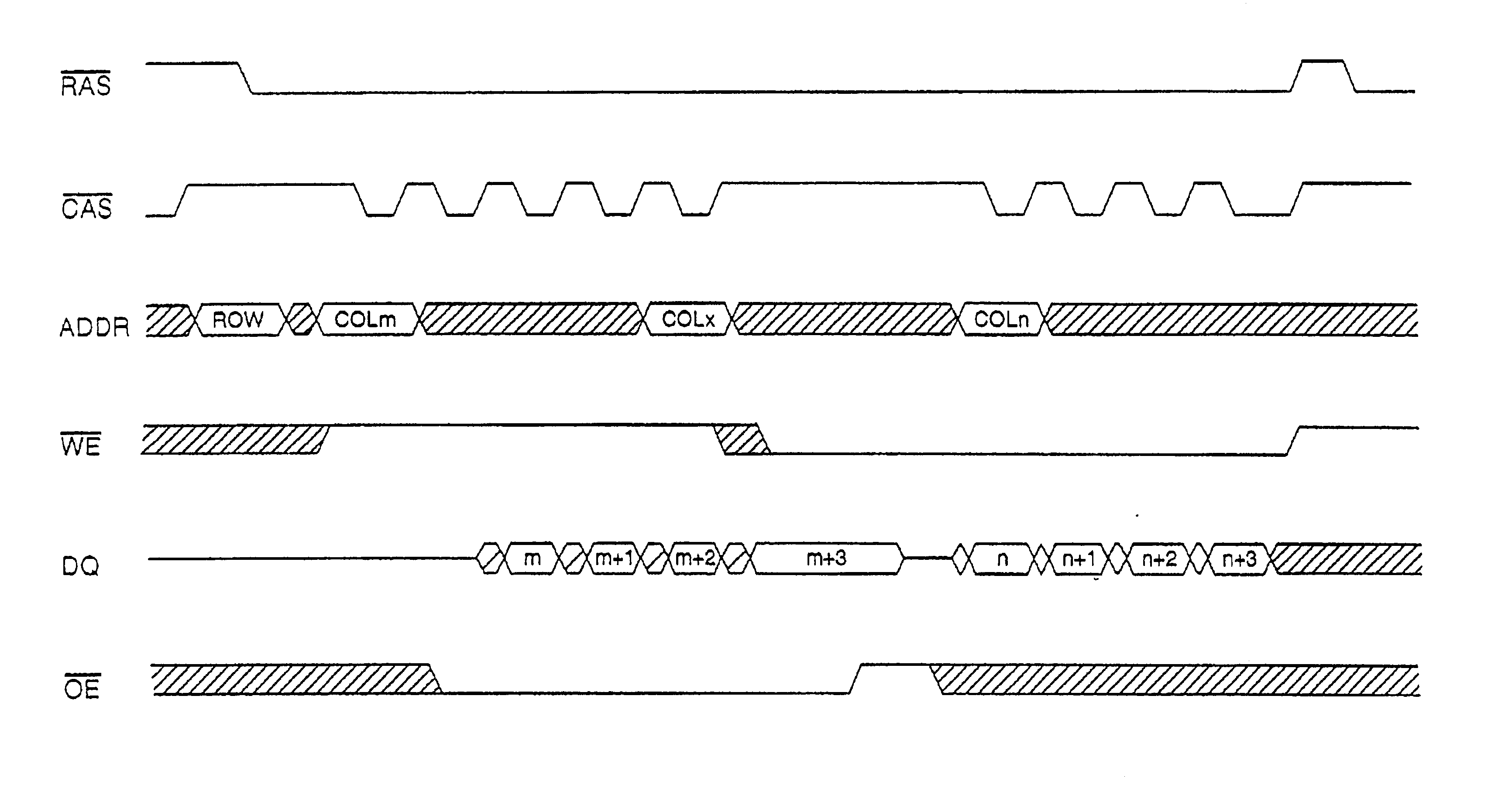
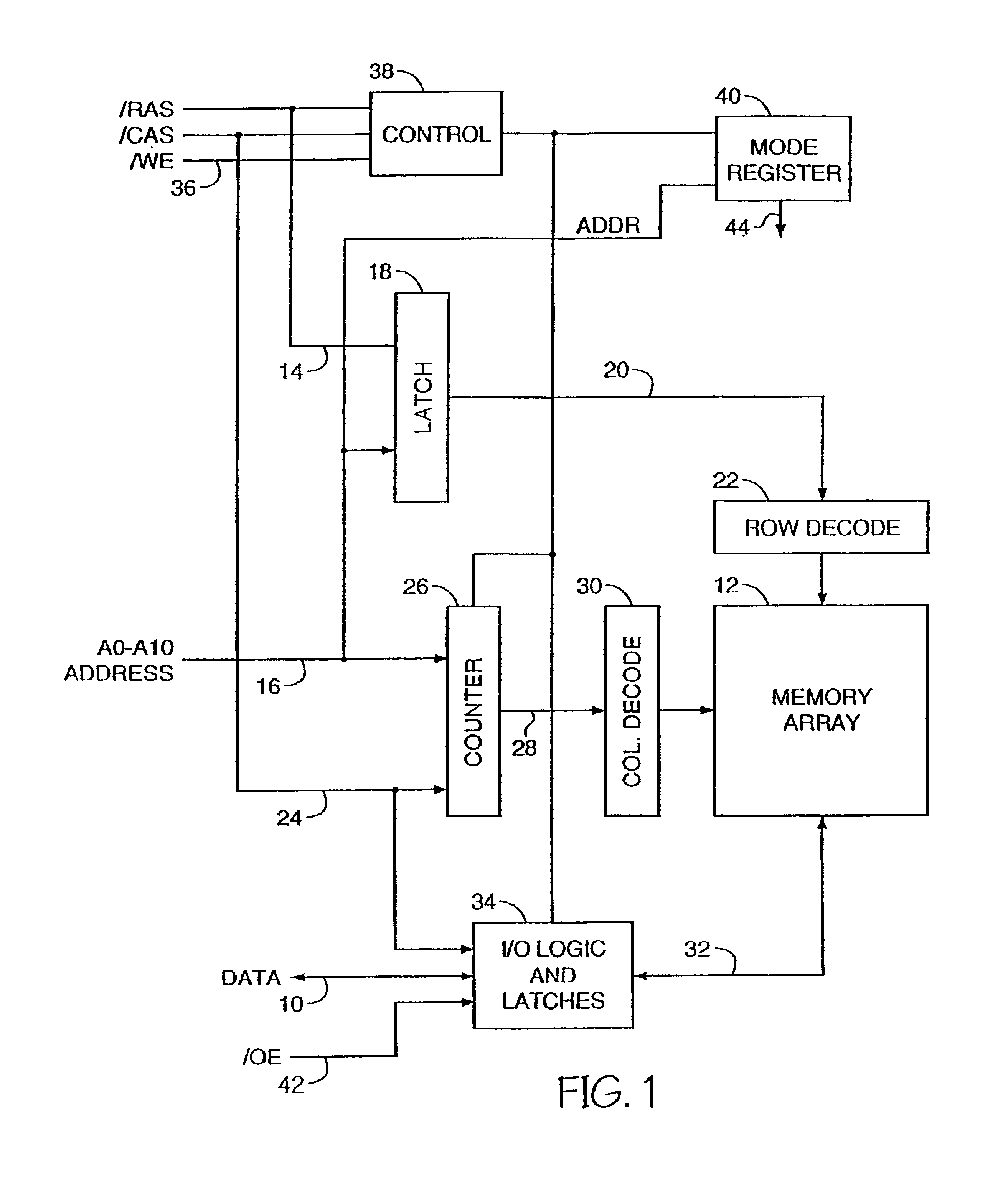
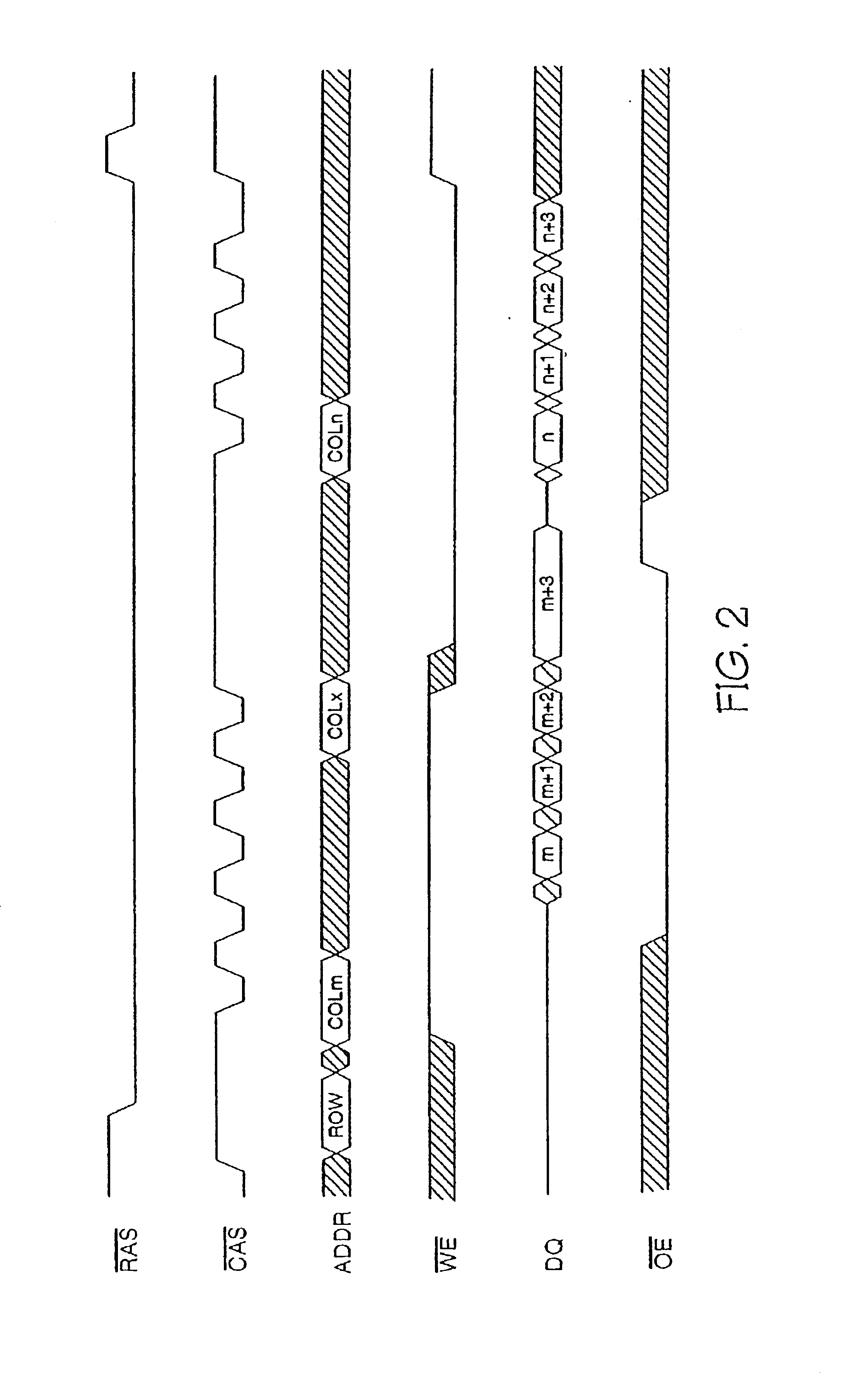
[0020]FIG. 1 is a schematic representation of a sixteen megabit device designed in accordance with the present invention. The device is organized as a 2 Meg×8 burst EDO DRAM having an eight bit data input / output path 10 providing data storage for 2,097,152 bytes of information in the memory array 12. The device of FIG. 1 has an industry standard pinout for eight bit wide EDO DRAMs. An active-low row address strobe ( / RAS) signal 14 is used to latch a first portion of a multiplexed memory address, from address inputs A0 through A1016, in latch 18. The latched row address 20 is decoded in row decoder 22. The decoded row address is used to select a row of the memory array 12. A column address strobe ( / CAS) signal 24 is used to latch a second portion of a memory address from address inputs 16 into column address counter 26. The latched column address 28 is decoded in column address decoder 30. The decoded column address is used to select a column of the memory array 12.

[0021]In a burst r...


PUM


Abstract

An integrated circuit memory device is designed to perform high speed data write cycles. An address strobe signal is used to latch a first address. During a burst access cycle the address is incremented internal to the device with additional address strobe transitions. A new memory address is only required at the beginning of each burst access. Read / Write commands are issued once per burst access eliminating the need to toggle the Read / Write control line at the device cycle frequency. A transition of the Read / Write control line during a burst access is used to terminate the burst access and initialize the device for another burst access. Write cycle times are maximized to allow for increases in burst mode operating frequencies. Local logic gates near array sense amplifiers are used to control write data drivers to provide for maximum write times without crossing current during input / output line equilibration periods. By gating global write enable signals with global equilibrate signals locally at data sense amp locations, local write cycle control signals are provided which are valid for essentially the entire cycle time minus an I / O line equilibration period in burst access memory devices. For nonburst mode memory devices such as EDO and Fast Page Mode, the write function may begin immediately following the end of the equilibration cycle to provide a maximum write time without interfering with the address setup time of the next access cycle.

Description

CROSS REFERENCE TO RELATED APPLICATIONS[0001]This application is a division of U.S. patent application Ser. No. 09 / 361,795, filed on Jul. 27, 1999, which in turn is a continuation of U.S. patent application Ser. No. 09 / 031,325, filed on Feb. 26, 1998, which is a division of U.S. patent application Ser. No. 08 / 785,867, filed on Jan. 21, 1997, now U.S. Pat. No. 5,757,703, which is a continuation of U.S. patent application Ser. No. 08 / 497,354, filed on Jun. 30, 1995, now issued as U.S. Pat. No. 5,598,376, which is a continuation-in-part of U.S. patent application Ser. No. 08 / 386,894, filed on Feb. 10, 1995, now issued as U.S. Pat. No. 5,610,864, which is a continuation-in-part of U.S. patent application Ser. No. 08 / 370,761, filed on Dec. 23, 1994, now issued as U.S. Pat. No. 5,526,320, the specifications of which are incorporated herein by reference.FIELD OF THE INVENTION[0002]This invention relates to memory device architectures designed to provide high density data storage with high ...

Claims


Application Information

Patent Timeline
Patent Type & Authority Patents(United States)
IPC IPC(8): G11C8/18G11C8/00G06F12/06G11C7/10G11C7/22G11C11/407
CPCG06F12/0638G11C11/4096G11C7/1021G11C7/1024G11C7/1027G11C7/1039G11C7/1045G11C7/1048G11C7/1078G11C7/109G11C7/1096G11C7/22G11C11/407G11C11/4076G06F2212/2022
Inventor MERRITT, TODD A.MANNING, TROY A.
Owner ROUND ROCK RES LLC
Why Eureka
Try Eureka