
Method for testing semiconductor devices having built-in self repair (BISR) memory

a technology of self-repair and memory, which is applied in the direction of information storage, static storage, instruments, etc., can solve the problems of high manufacturing difficulty, large test development cost, and high cost of asic development, and achieves high test development cos

Inactive Publication Date: 2006-07-11
BROADCOM INT PTE LTD
View PDF6 Cites 24 Cited by
  • Summary
  • Abstract
  • Description
  • Claims
  • Application Information

AI Technical Summary

Benefits of technology

[0010]In accordance with principles of the present invention, a method for testing a semiconductor device is disclosed. The method includes generating memory repair data for a wafer die by writing at least one predetermined digital bit pattern into a memory on the wafer die, reading the at least one predetermined digital bit pattern back out of the memory, comparing the at least one predetermined digital bit pattern read out from the memory against the at least one predetermined digital bit pattern written into the memory, and storing results of the comparison as the memory repair data. The writing and reading are performed a plurality of times, each time with a different voltage and clock frequency combination being applied to the circuit on the wafer die. The memory repair data is programmed...

Problems solved by technology

Because of the increasing complexity of new designs, test development costs can account for a large percentage of the total ASIC development cost.
This testing is necessary because perfect yields are difficult to achieve.
It is not uncommon for a certain percentage of unpackaged ASIC die to contain memory cells which fail testing processes, due largely to non-systemic manufacturing defects and degradation faults.
Such manufacturing issues are likely to increase as process geometries continue to shrink and the density of memory cells increases.

Method used


Image

  • Method for testing semiconductor devices having built-in self repair (BISR) memory
  • Method for testing semiconductor devices having built-in self repair (BISR) memory
  • Method for testing semiconductor devices having built-in self repair (BISR) memory

Examples


Embodiment Construction

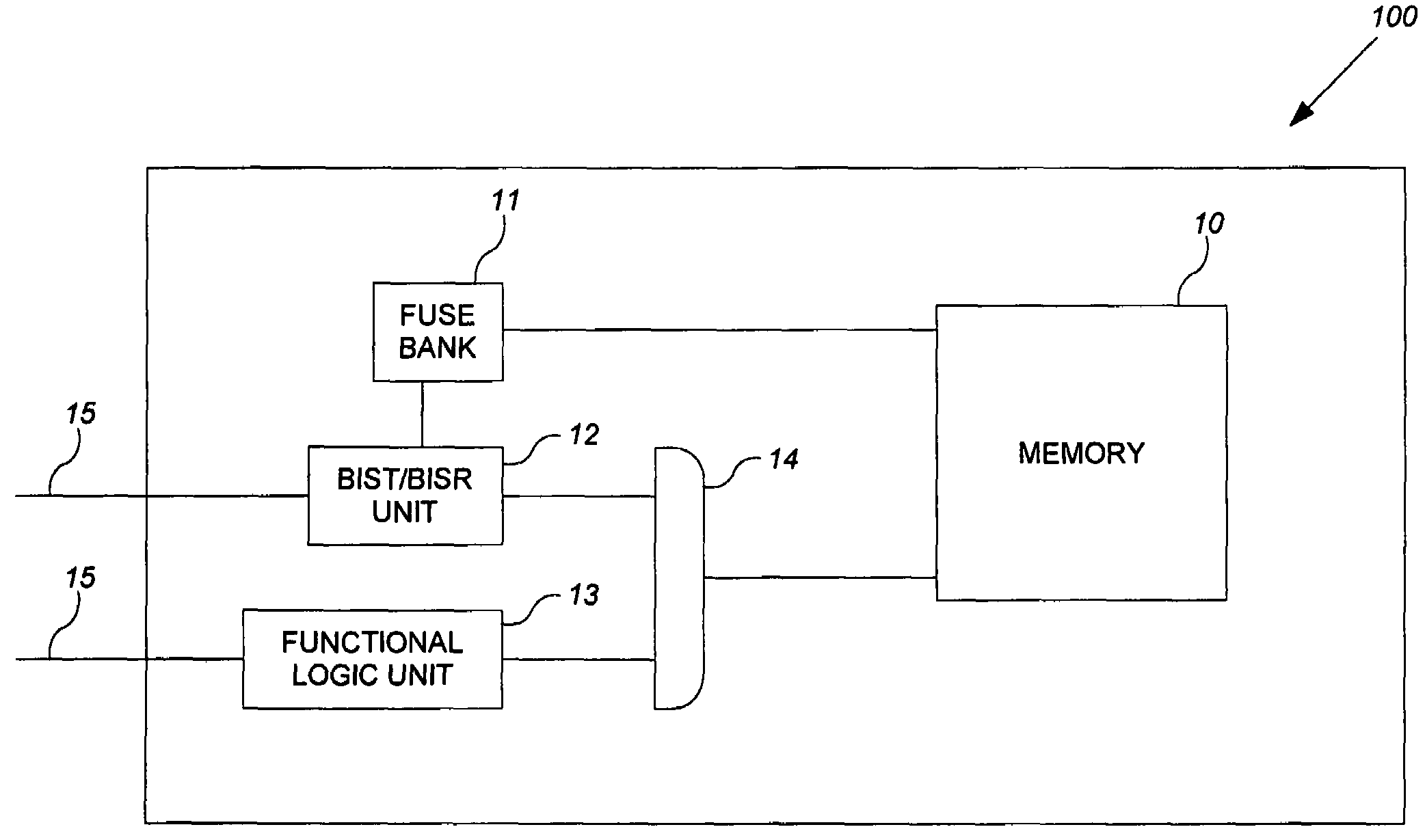
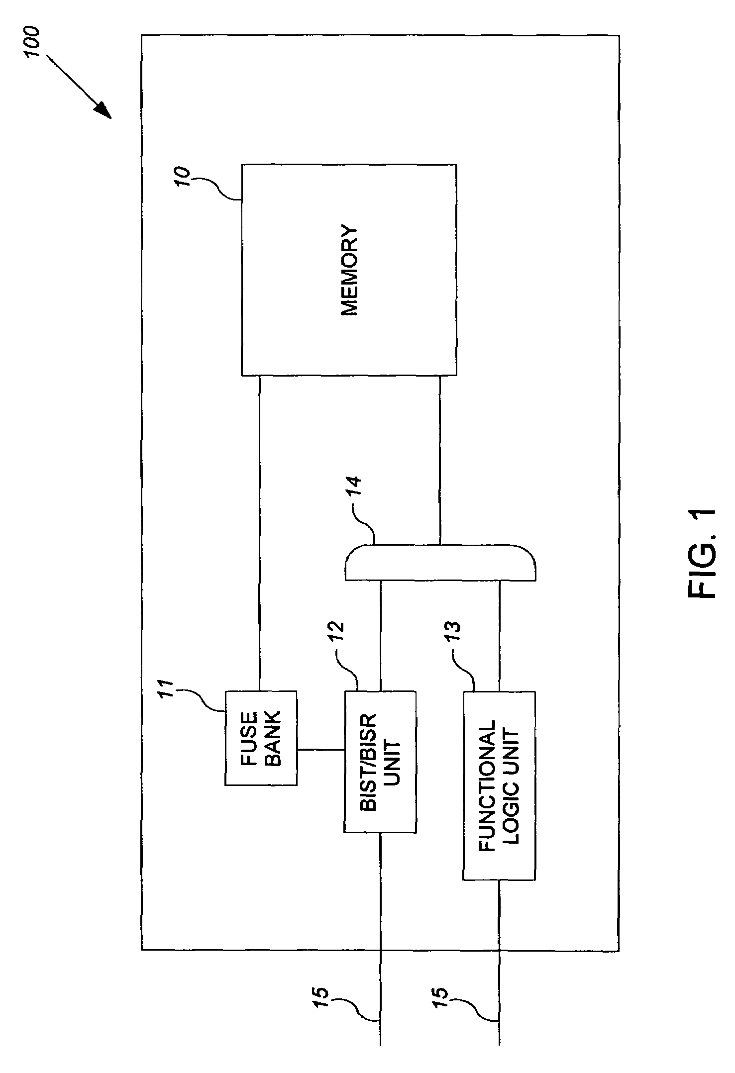
[0018]Referring now to the drawings, and more particularly to FIG. 1, a schematic diagram of an exemplary semiconductor device 100 having BISR memory is shown. In FIG. 1, the semiconductor device 100 comprises a memory 10, a fuse bank 11, a BIST / BISR unit 12, a functional logic unit 13, a multiplexer 14, and input / output terminals 15. For purposes of simplicity, the semiconductor device 100 of FIG. 1 is shown as having only one memory. However, in practice it is contemplated that the semiconductor device 100 may include a plurality of such memories, and other components including some not shown in FIG. 1. Also, the semiconductor device 100 is represented in FIG. 1 in an assembled and packaged form. Prior to assembly and packaging, however, the semiconductor device 100 is embodied as a wafer die that includes the components shown in FIG. 1. Accordingly, reference herein to a “wafer die” or simply “die” refers to a semiconductor device prior to its assembly into a packaged semiconduct...


PUM


Abstract

A method for testing semiconductor devices advantageously increases manufacturing yields. The method includes generating memory repair data for a wafer die by writing at least one predetermined digital bit pattern into a memory on the wafer die, reading the at least one predetermined digital bit pattern back out of the memory, comparing the at least one predetermined digital bit pattern read out from the memory against the at least one predetermined digital bit pattern written into the memory, and storing results of the comparison as the memory repair data. The writing and reading are performed a plurality of times, each time with a different voltage and clock frequency combination being applied to the wafer die. The memory repair data is programmed into the wafer die, and the wafer die is assembled into a packaged semiconductor device. The packaged semiconductor device is tested by causing the memory repair data programmed within the packaged semiconductor device to be transferred into the memory a plurality of times, each time with a different voltage and clock frequency combination being applied to the packaged semiconductor device.

Description

BACKGROUND OF THE INVENTION[0001]1. Field of the Invention[0002]The present invention generally relates to semiconductor memory devices, and more particularly, to a process suitable for testing semiconductor devices having built-in self repair (BISR) memory.[0003]2. Background Information[0004]Integrated circuits have become key components of many consumer and commercial electronic products, often replacing discrete components and enhancing functionality. The semiconductor processing technologies that produce these integrated circuits have advanced to the point where complete systems, including memories, can be reduced to a single integrated circuit or application specific integrated circuit (ASIC) device. It is a common practice for the manufacturers of such integrated circuits to thoroughly test device functionality at the manufacturing site. Because of the increasing complexity of new designs, test development costs can account for a large percentage of the total ASIC development...

Claims


Application Information

Patent Timeline
IPC IPC(8): G11C29/00
CPCG11C17/165G11C29/027G11C29/12015G11C29/44G11C29/50G11C29/50012G11C29/50016G11C29/4401G11C2029/4402
Inventor PURI, MUKESH K.AGRAWAL, GHASI R.SCHWARZ, WILLIAM
Owner BROADCOM INT PTE LTD
Learn More