
Electrophotographic photoreceptor and method for producing the same

a photoreceptor and electrophotographic technology, applied in the field of electrophotographic photoreceptors and a method for producing the same, can solve the problems of difficult correlation between the occurrence of interference fringes and surface roughness only with ry, ra, rz and sm, and achieve the effects of limiting the surface roughness of a conductive substrate, interference fringes, and high precision

Inactive Publication Date: 2006-07-18
SHARP KK
View PDF5 Cites 8 Cited by
  • Summary
  • Abstract
  • Description
  • Claims
  • Application Information

AI Technical Summary

Benefits of technology

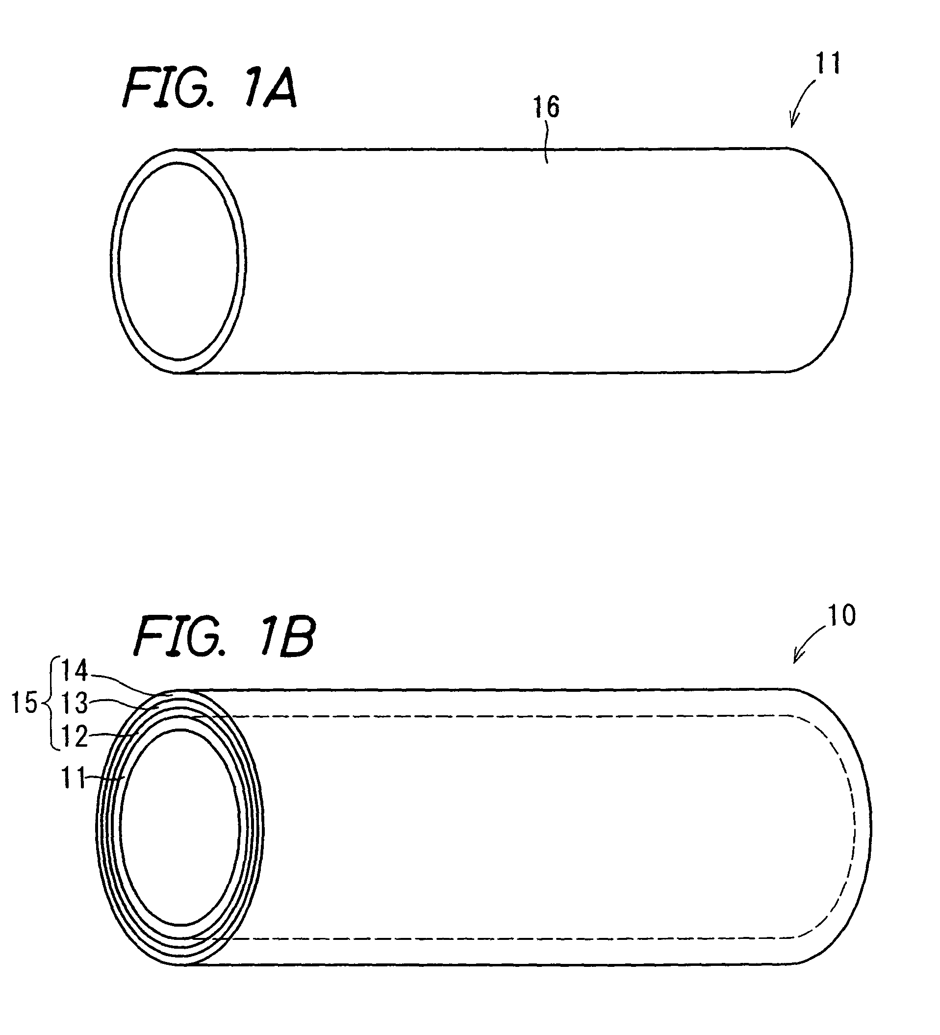
[0026]An object of the invention is to provide an electrophotographic photoreceptor in which interference fringes of images are prevented from occurring by limiting the surface roughness of a conductive substrate and the thickness of the layer can be measured with high precision by optical interferometry, and a method for producing the same.
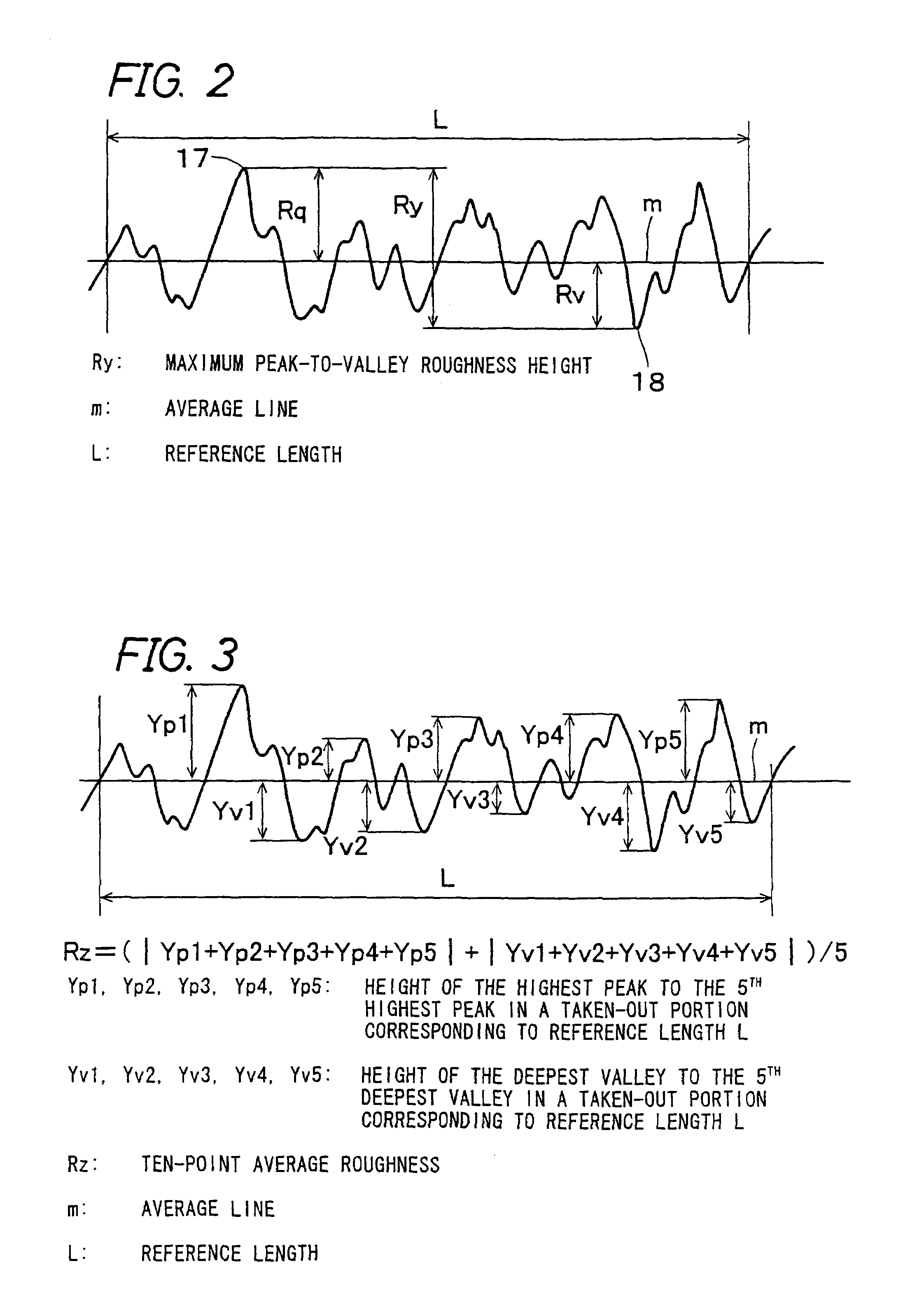
[0028]That is to say, it is known that the interference fringes (dark and light stripes in images) caused by multiple reflection in the photosensitive layer in an electrophotographic process using coherent light are affected by the surface roughness of the substrate and the fine waveform shape, and an effect of suppressing occurrence of the interference fringes can be obtained by setting Ry, Ra, Rz and Sm of the substrate surface to a predetermined size (roughness) or more to make the surface be rough.
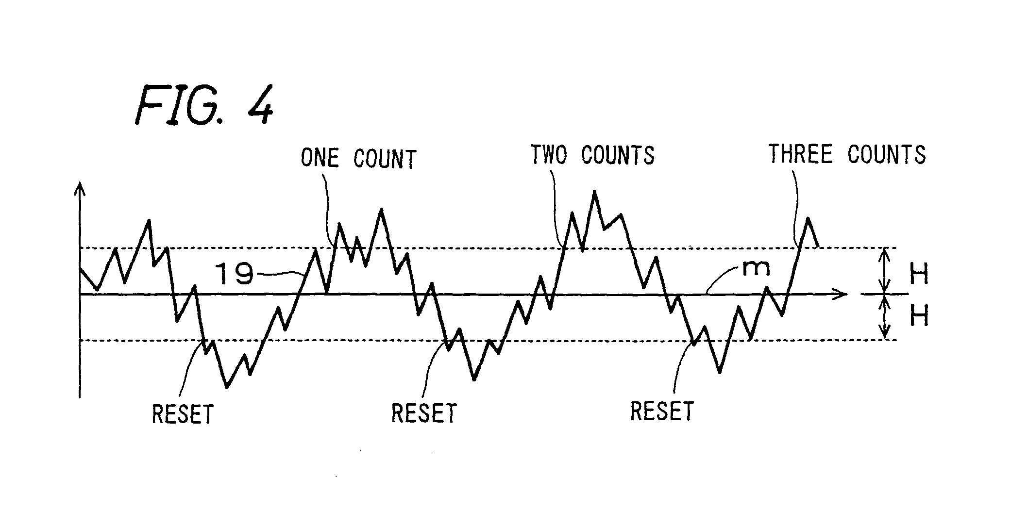
[0029]However, for interference fringes occurring in the images formed in an image forming apparatus having a small light spot, it is difficult to correlate the occurrence of the interference fringes and the surface roughness only with Ry, Ra, Rz and Sm. However, in addition to Ry, Ra, Rz and Sm, a peak count Pc obtained by counting the number of peaks having a height equal to or more than a predetermined width from the top point to the bottom point in the reference length that is the predetermined measurement distance is introduced, so that the correlation between the occurrence of the interference fringes and the surface roughness can be clarified. Moreover, the occurrence of the interference fringes is prevented by limiting Ry, Ra, Rz, Sm and Pc to be within a preferable range, so that it is possible to measure the thickness of the layer with high precision by the optical interferometry in an area having a rough surface roughness. The inventors of the invention obtained this knowledge and arrived at the invention.
[0038]According to the invention, the surface roughness of the conductive substrate of the electrophotographic photoreceptor can be limited to the preferable range using Pc as well as Ry, Ra, Rz, and Sm as the indices thereof. This realizes an electrophotographic photoreceptor in which inference fringes of the images caused by the multiple-reflection of light in the photosensitive layer formed on the conductive substrate can be prevented from occurring, and the thickness of the layer can be measured by the optical interferometry with high precision. Herein, the peak count Pc is an index of the surface roughness according to a parameter PPI defined in J911-1986 of the Society of Automotive Engineers (SAE) Standard and is a value obtained by counting the number of peaks having a height of at least the predetermined width of the top point and the bottom point in the reference length as described above.
[0050]According to the invention, the conductive substrate whose surface roughness is limited to the preferable range using Pc as well as Ry, Ra, Rz, and Sm as the indices of the surface roughness is prepared, the thickness of the layers is measured by optical interferometry when the coating is performed to form the layers constituting the photosensitive layer on the conductive substrate, measurement results are fed back, and an electrophotographic photoreceptor is produced while the thickness of the layers are adjusted. Thus, the surface roughness of the conductive substrate is in the preferable range and the thickness of the layers can be measured with good precision by optical interferometry, so that when coating and forming the layers constituting the photosensitive layer, the thickness of the layers can be formed stably, and non-uniformity in the thickness can be prevented. Furthermore, an electrophotographic photoreceptor can be produced in which the thickness precision of the photosensitive layer is excellent, and interference fringes do not occur.
[0052]According to the invention, the image forming apparatus includes the electrophotographic photoreceptor having the conductive substrate whose surface roughness is limited to the preferable range using Pc as well as Ry, Ra, Rz, and Sm as the indices of the surface roughness and the exposure apparatus that performs image-exposure on the surface of the electrophotographic photoreceptor at a pixel density of 1200 dpi or more so as to form electrostatic latent images. Thus, electrostatic latent images can be formed on the electrophotographic photoreceptor including the conductive substrate having the preferable surface roughness with light having a small spot diameter, so that an image forming apparatus can be realized in which inference fringes of images can be prevented from occurring, and high resolution and good quality images can be formed.

Problems solved by technology

However, for interference fringes occurring in the images formed in an image forming apparatus having a small light spot, it is difficult to correlate the occurrence of the interference fringes and the surface roughness only with Ry, Ra, Rz and Sm.

Method used


Image

  • Electrophotographic photoreceptor and method for producing the same
  • Electrophotographic photoreceptor and method for producing the same
  • Electrophotographic photoreceptor and method for producing the same

Examples


examples

[0120]Hereinafter, examples of the invention will be described. However, the invention is not limited to the examples.

examples 1 to 11

[0121]A cylindrical conductive substrate made of aluminum having a diameter of 30 mm, a thickness of 0.75 mm and a length of 322.3 mm was prepared. The outer circumferential surface of this cylindrical conductive substrate made of aluminum is cut and processed with a diamond cutting tool while varying the shape of the blade of the cutting tool, the travel speed of the cutting tool, the type of a lubricant and the like. In this manner, the surface was finished such that the surface roughness was in the range of the invention: (a) the maximum peak-to-valley roughness height Ry: 0.8 to 1.4 μm, (b) the centerline average roughness Ra: 0.10 to 0.15 μm, (c) the ten-point average roughness Rz: 0.7 to 1.3 μm, (d) the average peak-to-peak distance Sm: 5 to 30 μm, and (e) the peak count Pc: 60 to 100. The surface roughness of the cut and processed conductive substrate, that is, (a) to (e) were measured with a surface roughness meter SURFCOM 570A (manufactured by Tokyo Seimitsu Co. Ltd.).

[0122...


PUM

PropertyMeasurementUnit
wavelengthaaaaaaaaaa
heightaaaaaaaaaa
Raaaaaaaaaaa

Abstract

The object of the invention is to prevent interference fringes of images and allow precise measurement of the thickness of a layer by the optical interferometry by limiting the surface roughness of a conductive substrate. The surface roughness of the conductive substrate provided in an electrophotographic photoreceptor is such that the maximum peak-to-valley roughness height (Ry)=0.8 to 1.4 μm, the centerline average roughness (Ra)=0.10 to 0.15 μm, the ten-point average roughness (Rz)=0.7 to 1.3 μm, the average peak-to-peak distance (Sm)=5 to 30 μm, and the peak count Pc=60 to 100. In such an electrophotographic photoreceptor, light for exposure can be scattered to an appropriate extent, so that interference fringes can be prevented, and an interference pattern is formed during measurement of the thickness of the photosensitive layer by the optical interferometry so that the thickness of the layer can be measured with a high precision.

Description

BACKGROUND OF THE INVENTION[0001]1. Field of the Invention[0002]The present invention relates to an electrophotographic photoreceptor and a method for producing the same.[0003]2. Description of the Related Art[0004]Conventionally, in an electrophotographic image forming process in an electrophotographic application apparatus such as copiers and laser printers, gas lasers having a comparatively short wavelength such as He—Ne lasers, Ar lasers, and He—Cd lasers have been used as light to which a surface of an electrophotographic photoreceptor is exposed so as to form electrostatic latent images. CdS, ZnO, Se or the like, which forms a thick layer, has been used for a photosensitive layer of an electrophotographic photoreceptor that can be used with such a gas laser. Therefore, light for exposure with which the electrophotographic photoreceptor is irradiated by the gas laser is completely absorbed by the thick photosensitive layer, so that interference caused by reflection on the subst...

Claims


Application Information

Patent Timeline
Patent Type & Authority Patents(United States)
IPC IPC(8): G03G5/10G03G21/00G03G5/05
CPCG03G5/10
Inventor HASHIMOTO, MASAKIMORITA, KAZUSHIGEKAKUI, MIKIOTANAKA, YUJISAKAMOTO, MASAYUKI
Owner SHARP KK
Learn More