
Vertical unipolar component

a technology of vertical unipolar components and components, applied in the direction of transistors, electrical devices, solid-state devices, etc., can solve the problems of complex structure manufacturing, and achieve the effect of high breakdown voltage and simple manufacturing of the structure of the figur

Active Publication Date: 2006-07-18
STMICROELECTRONICS SRL
View PDF6 Cites 13 Cited by
  • Summary
  • Abstract
  • Description
  • Claims
  • Application Information

AI Technical Summary

Benefits of technology

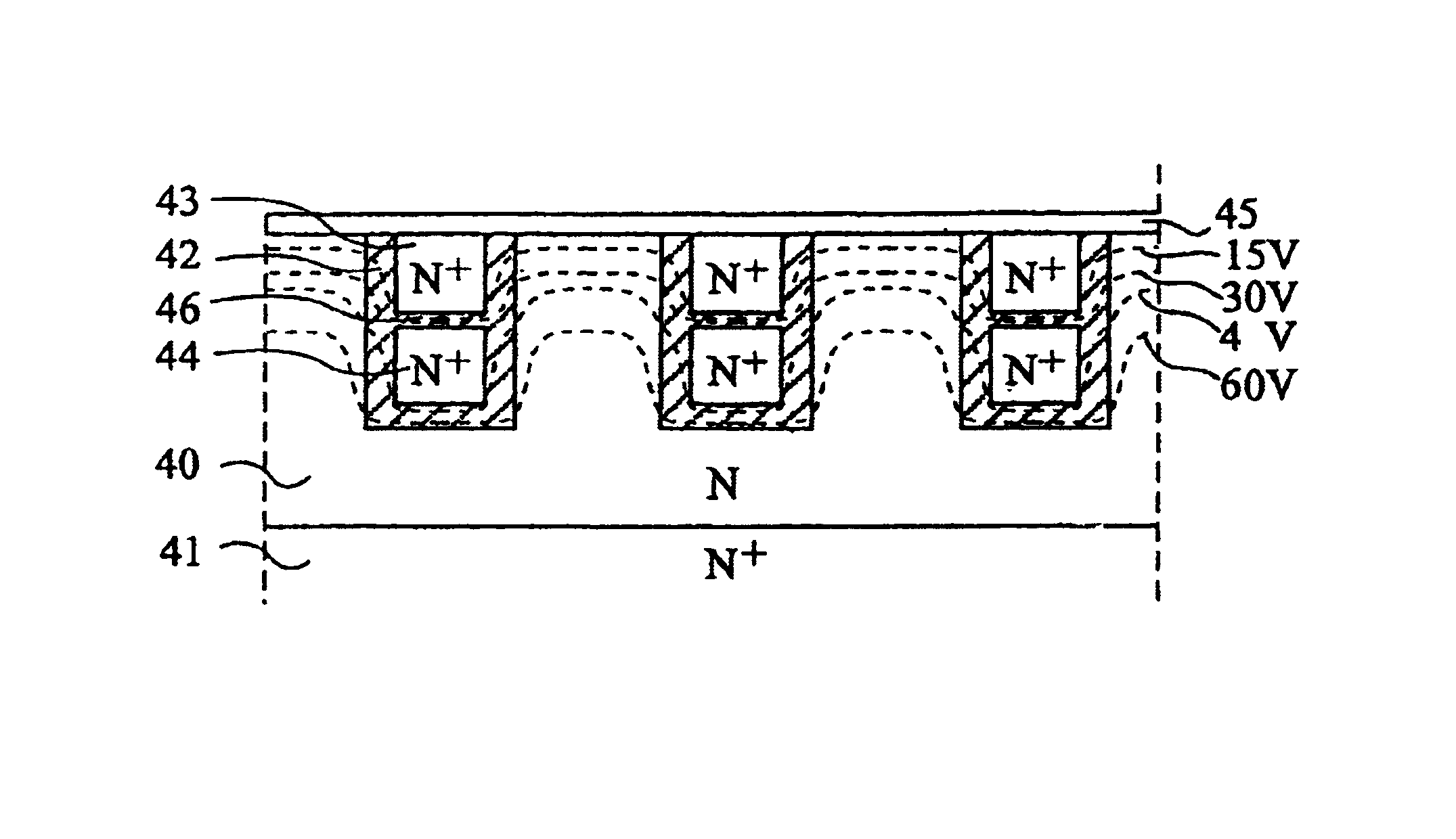
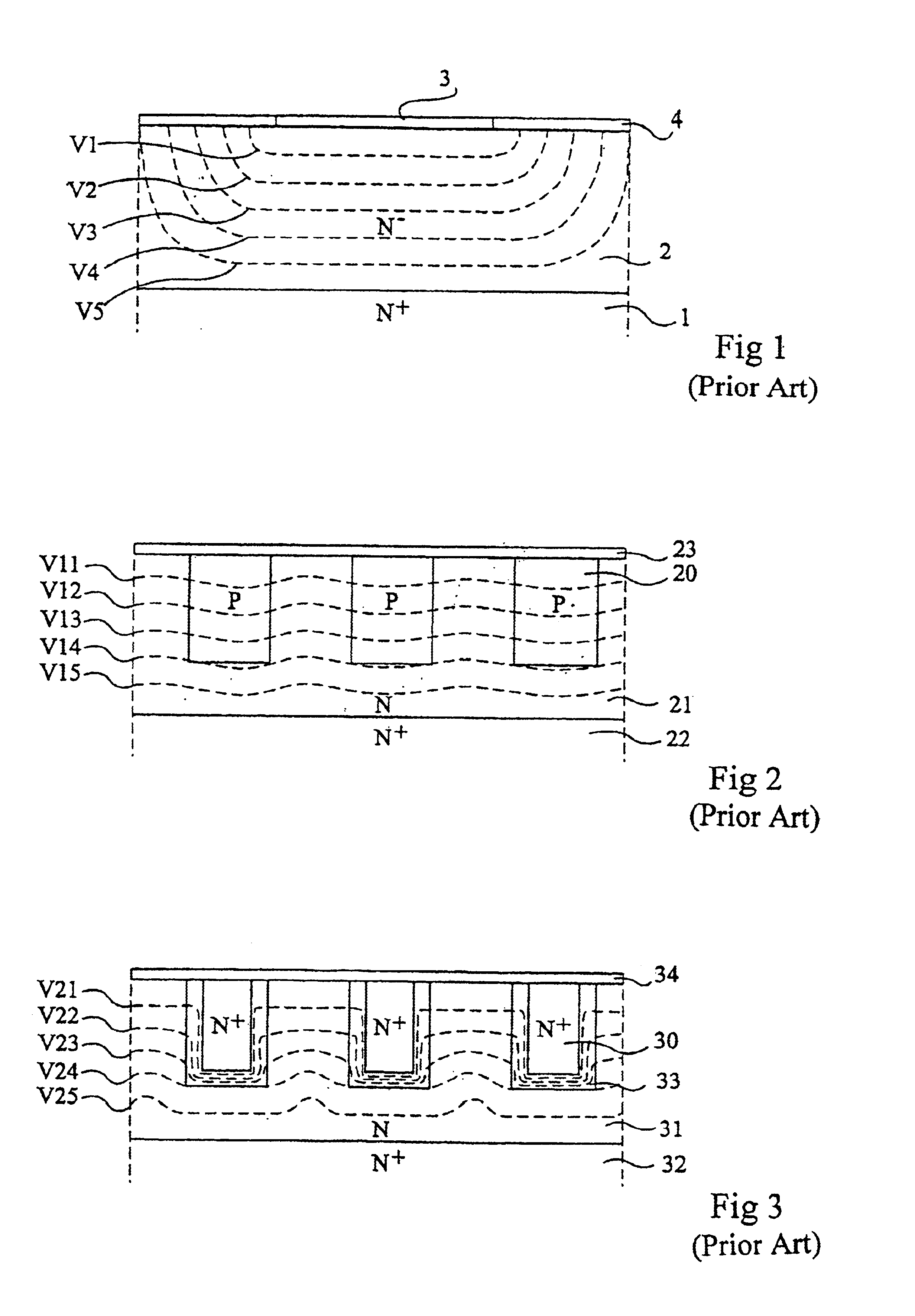
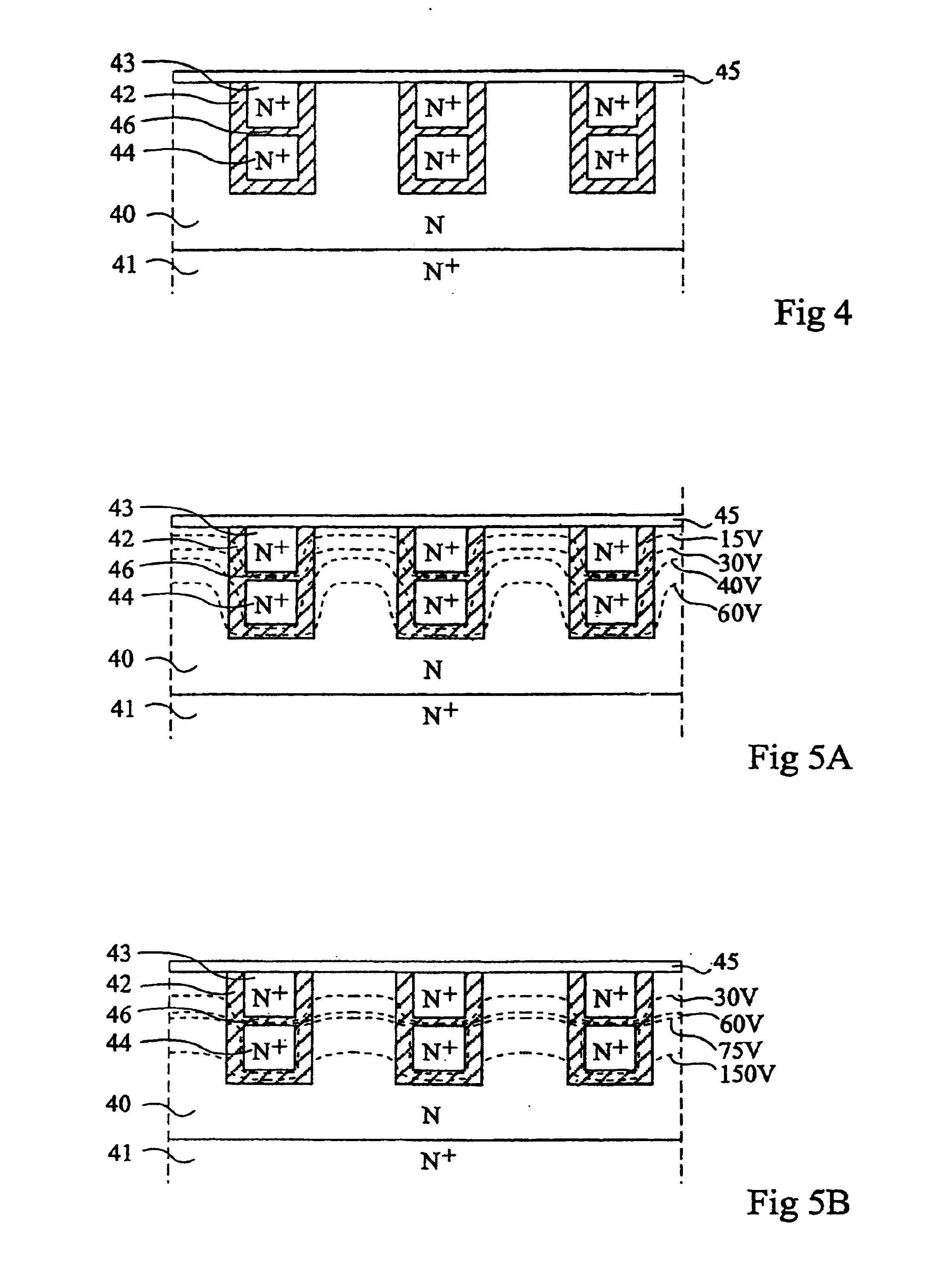
[0017]The present invention aims at a unipolar component structure which overcomes the disadvantages of known structures, that is, which has both the advantage of a high breakdown voltage of the structure of FIG. 2 and the advantage of the manufacturing simplicity of the structure of FIG. 3.

Problems solved by technology

However, such a structure is complex to manufacture.

Method used


Image

  • Vertical unipolar component
  • Vertical unipolar component
  • Vertical unipolar component

Examples


Embodiment Construction

[0038]For clarity, the same elements have been referred to with the same reference numerals in the different drawings. Further, as usual in semiconductor component representation, the drawings are not to scale.

[0039]FIG. 4 is a partial simplified cross-section view of an embodiment of a Schottky diode according to the present invention. The cathode of the diode is an upper portion (N) 40 of a semiconductor substrate, for example made of single-crystal silicon. A lower portion (N+) 41 of the substrate forms a contact area of the cathode. Cathode 40 is more lightly doped than portion 41.

[0040]In cathode 40 are formed trenches coated with an insulator 42 and filled with a conductor divided in two conductive elements, a high element 43 and a low element 44 separated by an insulating layer 46. It will be said hereafter that insulated conductor elements 43-44 form a multiple-layer. The upper surface of high element 43 is coplanar with the upper surface of peripheral cathode 40 and is also...


PUM


Abstract

A vertical unipolar component formed in a semiconductor substrate. An upper portion of the substrate includes insulated trenches filled with a vertical multiple-layer of at least two conductive elements separated by an insulating layer, the multiple-layer depth being at most equal to the thickness of the upper portion.

Description

BACKGROUND OF THE INVENTION[0001]1. Field of the Invention[0002]The present invention relates to the manufacturing of vertical unipolar components in monolithic form. The following description more specifically aims, as an example only, at the case of components of Schottky diode type made in vertical form in silicon substrates.[0003]2. Discussion of the Related Art[0004]FIG. 1 illustrates a conventional structure of a Schottky diode. The structure comprises a heavily-doped semiconductor substrate (N+) 1, typically made of single-crystal silicon. A cathode layer (N−) 2 more lightly doped than substrate 1 covers substrate 1. A metal layer 3 forms a Schottky contact with cathode 2 and forms the diode anode. The contour of anode 3 is defined by an insulator 4.[0005]FIG. 1 also illustrates, in dotted lines, a distribution of equipotential surfaces V1, V2, V3, V4, and V5 in cathode 2 upon reverse biasing at a voltage V5. Equipotential surfaces V1 to V5 are equidistant, the intermediary e...

Claims


Application Information

Patent Timeline
Patent Type & Authority Patents(United States)
IPC IPC(8): H01L27/095H01L29/47H01L29/812H01L31/07H01L31/108H01L29/06H01L29/40H01L29/872
CPCH01L29/404H01L29/407H01L29/8725H01L29/872H01L29/7813
Inventor LANOIS, FREDERIC
Owner STMICROELECTRONICS SRL
Learn More