Interface controller using JTAG scan chain

Active Publication Date: 2006-07-18
ALTERA CORP
View PDF3 Cites 25 Cited by
  • Summary
  • Abstract
  • Description
  • Claims
  • Application Information

AI Technical Summary

Benefits of technology

[0016]This allows a user of the host computer system to transfer updated configuration data to the configuration memory device by means of a connection from the host computer system to the JTAG port of the programmable logic device. Since the user will in any event require a connection from the host computer system to t

Problems solved by technology

When a programmable logic device is supplied by a manufacturer, it is typically

Method used


Image

  • Interface controller using JTAG scan chain
  • Interface controller using JTAG scan chain
  • Interface controller using JTAG scan chain

Examples


Embodiment Construction

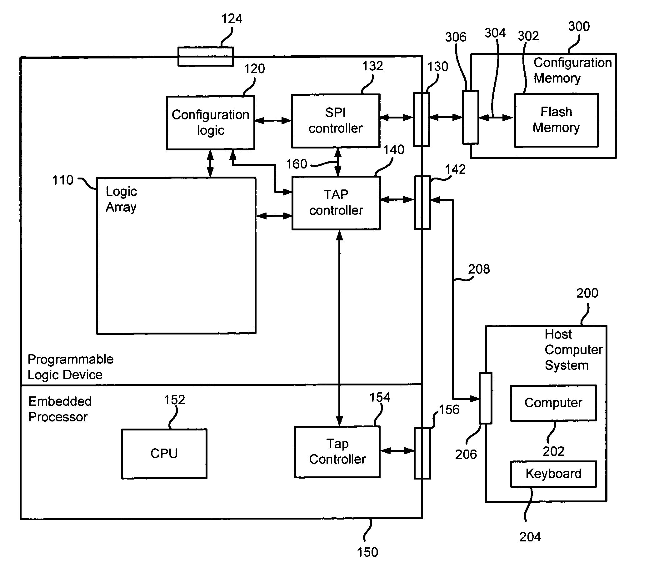
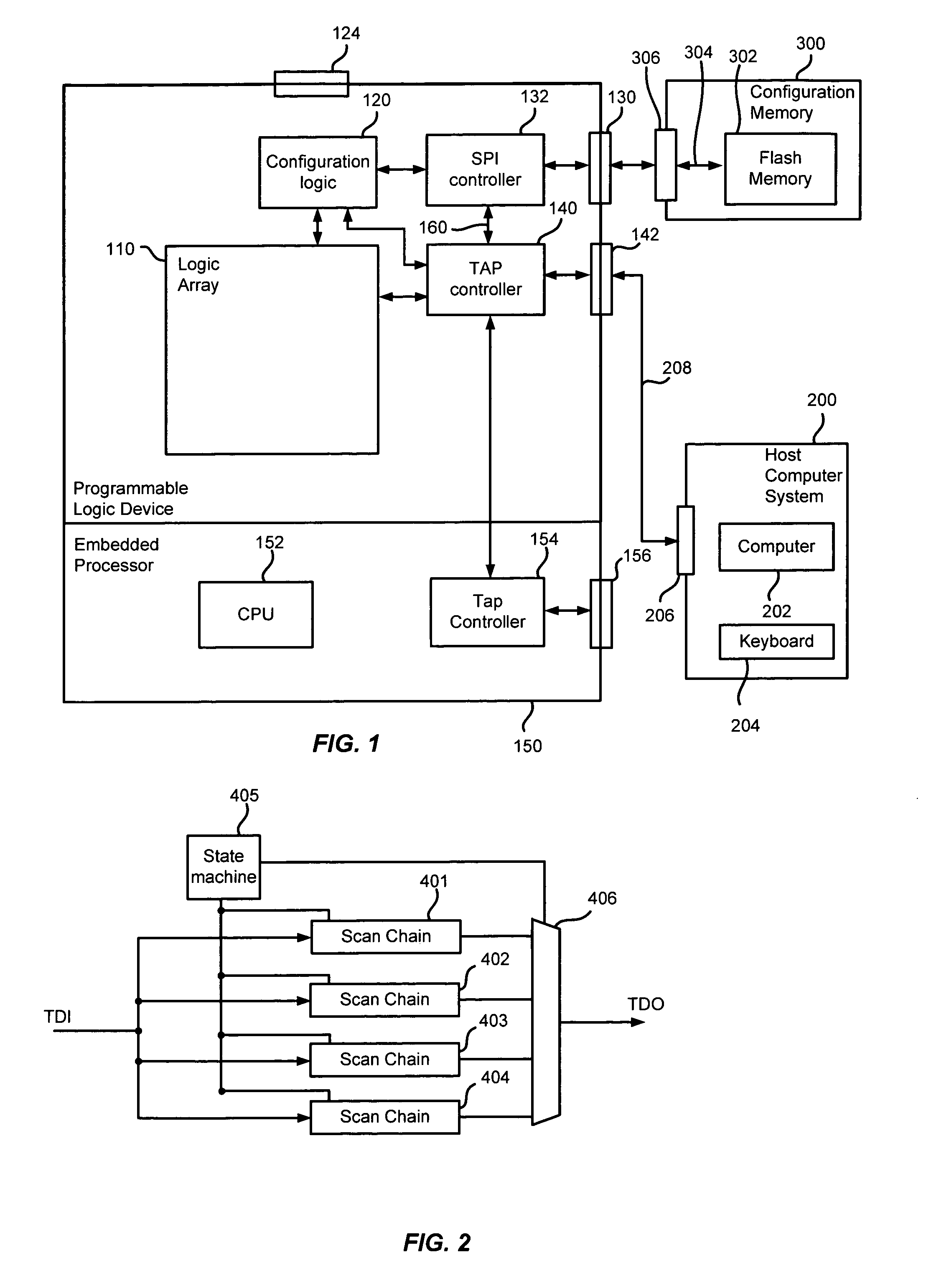
[0022]FIG. 1 is a block schematic diagram of a computer system, which includes a programmable logic device 100, in accordance with the present invention, a host computer system 200, and a configuration memory device 300.

[0023]The programmable logic device 100 is based around a logic array 110, which is made up of configurable logic array blocks, and configurable input-output devices, plus memory blocks and dedicated digital signal processing blocks. The structure of the logic array 110 is not shown in detail, as such structures are well known in themselves, and the details of the structure are not essential to an understanding of the present invention.

[0024]As mentioned above, the logic array 110 includes configurable logic array blocks, and configurable input-output devices. These elements perform functions which are assigned to them by configuration data. The configuration data is passed to the logic array 110 when required by means of a configuration logic block 120.

[0025]Configu...


PUM


Abstract

In a programmable logic device system, including a programmable logic device, a configuration memory device, for storing configuration information, and a host computer system, for generating updated configuration information, the programmable logic device has a JTAG port, for connection to said host computer system, for receiving said updated configuration information, a JTAG port controller, operatively connected to the first JTAG port, and an SPI interface, for connection to said configuration memory device. The JTAG port controller comprises a scan chain, for controlling said SPI interface on the basis of information received from said host computer system. This allows a user of the host computer system to transfer updated configuration data to the configuration memory device by means of a connection from the host computer system to the JTAG port of the programmable logic device. Since the user will in any event require a connection from the host computer system to the JTAG port of the programmable logic device to allow testing of the device, this will avoid the need for the user to continually switch connections on the programmable logic device.

Description

BACKGROUND OF THE INVENTION[0001]This invention relates to integrated circuits, and in particular to the control of an interface of an integrated circuit.[0002]More particularly, the invention relates to a programmable logic device, and to a technique for controlling an interface of a programmable logic device.[0003]A programmable logic device is an integrated circuit, which can be customized by a circuit designer to perform different functions. When a programmable logic device is supplied by a manufacturer, it is typically not capable of performing any particular function, but must first be configured. Programmable logic devices generally comprise an array of logic blocks, which can be programmed to perform desired functions, and which can be arbitrarily connected to each other, and to the inputs and outputs of the device.[0004]The data required in order to program the logic blocks, and the interconnect structure which lies between the logic blocks, is typically stored in a separat...

Claims


Application Information

Patent Timeline
IPC IPC(8): H03K19/013G01R31/28
CPCG01R31/318555
Inventor DRAPER, ANDREWFLAHERTY, EDWARD
Owner ALTERA CORP
Why Eureka
Try Eureka