Compensating for aging in OLED devices
- Summary
- Abstract
- Description
- Claims
- Application Information
AI Technical Summary
Benefits of technology
Problems solved by technology
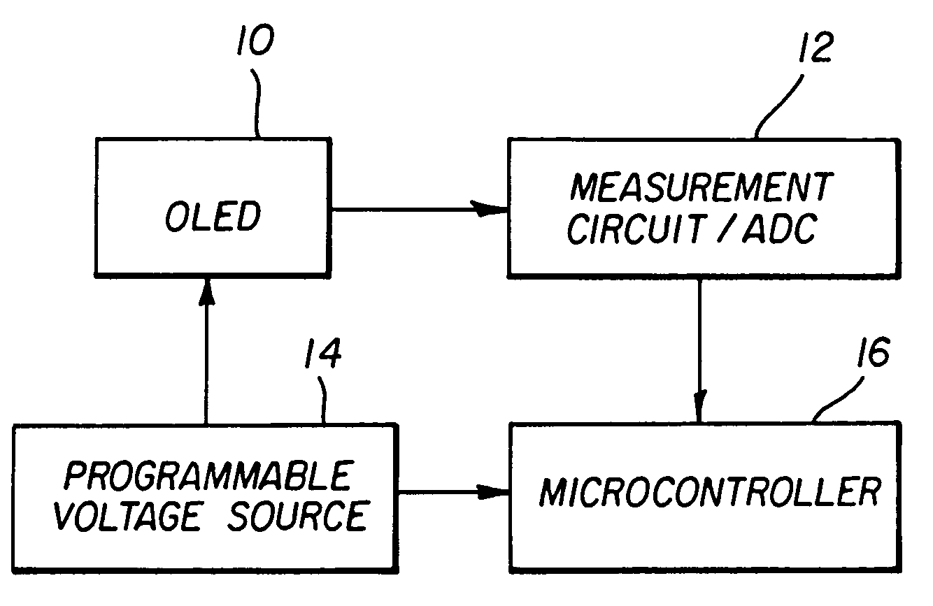
Method used
Image

Examples
Embodiment Construction
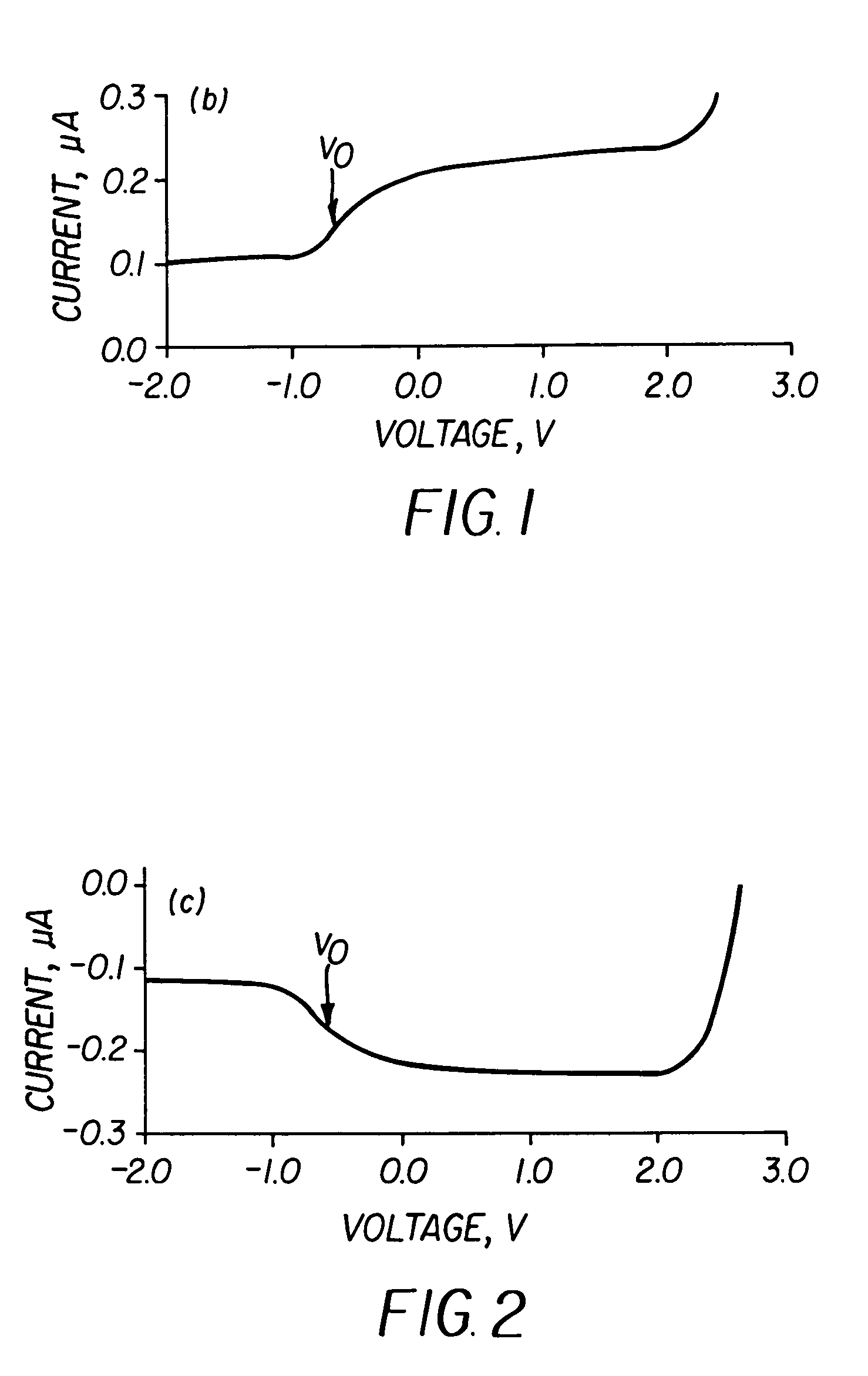
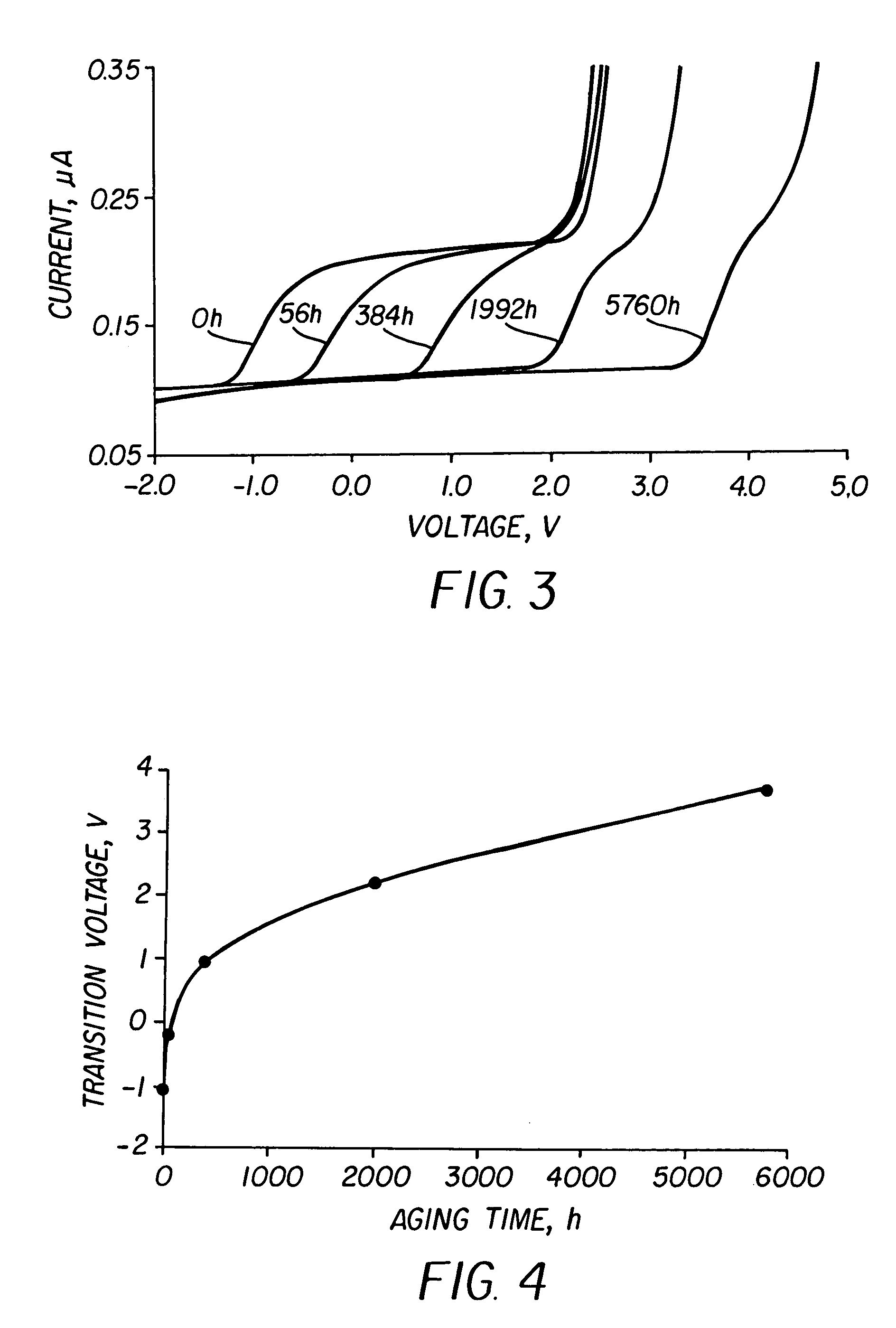
[0028]FIG. 1 shows linear sweep voltammogram, or linear-ramp current-voltage (I-V) measurements, of a typical ITO|NPB(750 Å)|Alq3(750 Å)|Mg:Ag OLED device. In this experiment, the applied voltage (V) is ramped at a constant rate, dV / dt, and the resulting current (I) is recorded. In general, the measured current has two components: a conductive component that would persist with a constant bias; and a capacitive component that is proportional to dV / dt and the differential capacitance. At sufficiently high scan rates (here, 50 V / s) and low applied voltages (here, ≦2.2 V), the current is dominated by the capacitive component. The transition voltage (V0), is operationally defined as inflection points on the I-V curve and identified with an arrow in FIG. 1. A second transition occurs at higher applied voltages, near Vbi, where the conductive component becomes dominant. The similar behavior above ˜2.2 V, regardless of the scan rate, confirms the identification of the transition near this v...
PUM
 Abstract
Description
Claims
Application Information