

Semiconductor memory device with back gate potential control circuit for transistor in memory cell
a technology of potential control circuit and memory cell, which is applied in the direction of screw threaded joints, instruments, mechanical equipment, etc., can solve the problems of inability to invert the held data, inability to consider a configuration for writing data at high speed, and increase current dissipation, so as to achieve high-speed and stable data reading and writing, and reduce current dissipation
- Summary
- Abstract
- Description
- Claims
- Application Information
AI Technical Summary
Benefits of technology
Problems solved by technology
Method used
Image

Examples
first embodiment
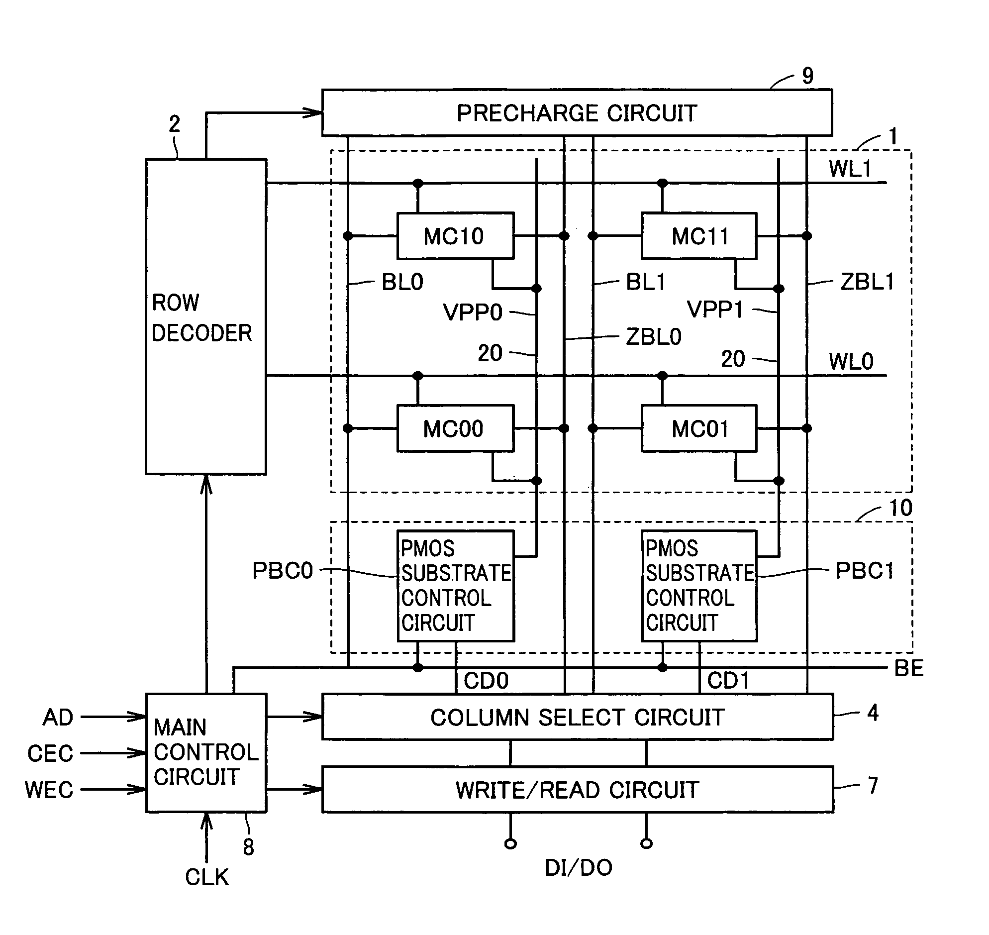
[0058]FIG. 1 schematically shows by way of example an overall configuration of the semiconductor memory device according to the present invention. FIG. 1 shows a configuration of a synchronous type single port SRAM that operates in synchronization with a clock signal. The configuration of the SRAM according to the present invention, however, is not limited thereto. It may be an SRAM operating in accordance with a chip select signal and asynchronously to the clock signal, or may be a dual port SRAM.
[0059]Referring to FIG. 1, the semiconductor memory device includes a memory cell array 1 having a plurality of memory cells arranged in rows and columns, a row decoder 2 for decoding an applied row address signal to generate a word line select signal, a column select circuit 4 for decoding an applied Y address signal to generate a column select signal CD for selecting a column of memory cell array 1 and connecting the selected column to an internal data line, a write / read circuit 7 perfor...
second embodiment
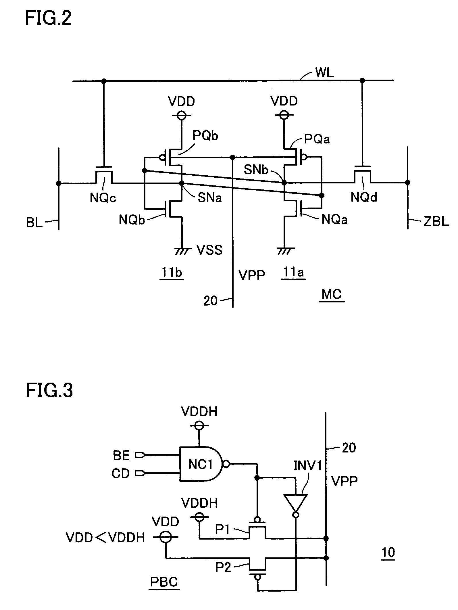
[0101]FIG. 5 shows a configuration of a PMOS substrate control circuit PBC according to a second embodiment of the present invention. The PMOS substrate control circuit PBC shown in FIG. 5 differs from PMOS substrate control circuit PBC shown in FIG. 3 in the following point. Specifically, P channel MOS transistor (pass transistor) P1 is coupled to a power supply node supplying power supply voltage VDD, and pass transistor P2 is coupled to a low voltage source node VDDL. The other configuration of the PMOS substrate control circuit PBC shown in FIG. 5 is identical with that of PMOS substrate control circuit PBC shown in FIG. 3, and the corresponding portions are denoted by the same reference characters, and detailed description thereof is not repeated.
[0102]The overall configuration of the semiconductor memory device is identical to that of the semiconductor memory device shown in FIG. 1. The memory cell configuration is also identical to the configuration shown in FIG. 2.
[0103]The ...
third embodiment
[0111]FIG. 7 shows a configuration of a PMOS substrate control circuit PBC according to a third embodiment of the present invention. In the configuration of substrate control circuit PBC shown in FIG. 7, pass transistor P1 transmits power supply voltage VDD to substrate voltage transmission line 20 in accordance with an output signal of NAND circuit NC1. Pass transistor P2 is coupled to receive power supply voltage VDD via a diode-connected P channel MOS transistor P3, and transmits a voltage VDD-Vtp transmitted via P channel MOS transistor P3 to substrate voltage transmission line 20 in accordance with an output signal of inverter INV1. Here, Vtp indicates an absolute value of the threshold voltage of P channel MOS transistor P3.
[0112]When the high voltage of substrate bias voltage VPP is power supply voltage VDD and therefore, is 1.0 V, the absolute value Vtp of the threshold voltage of P channel MOS transistor P3 is set to 0.5 V. In this case, the low voltage of substrate bias vo...
PUM
 Abstract
Description
Claims
Application Information