Solid state image pickup device and image pickup system

a pickup device and solid-state technology, applied in the field of solid-state image pickup devices and image pickup systems, can solve the problems of lowering the manufacturing yield of wiring and prone to arise, and achieve the effects of widening the design margin, reducing the number of lines, and improving manufacturing yield

Inactive Publication Date: 2006-07-25
CANON KK
View PDF18 Cites 29 Cited by
  • Summary
  • Abstract
  • Description
  • Claims
  • Application Information

AI Technical Summary

Benefits of technology

[0042]Thus, if the common usage of one line is effected, since a single common line will have the functions of a plurality of control lines, it is possible to reduce the number of lines in a solid image pickup device, thus widening the margin in design and remarkably improving manufacturing yield related to wiring.

Problems solved by technology

However, since the APS has a larger number of elements within one pixel (within one unit cell) as compared with the CCD image sensor, and since the size of a chip has been increased with the tendency of enlargement of the sensor area in recent years, a lowering in the manufacturing yield related to wiring is liable to arise.

Method used


Image

  • Solid state image pickup device and image pickup system
  • Solid state image pickup device and image pickup system
  • Solid state image pickup device and image pickup system

Examples


embodiment 1

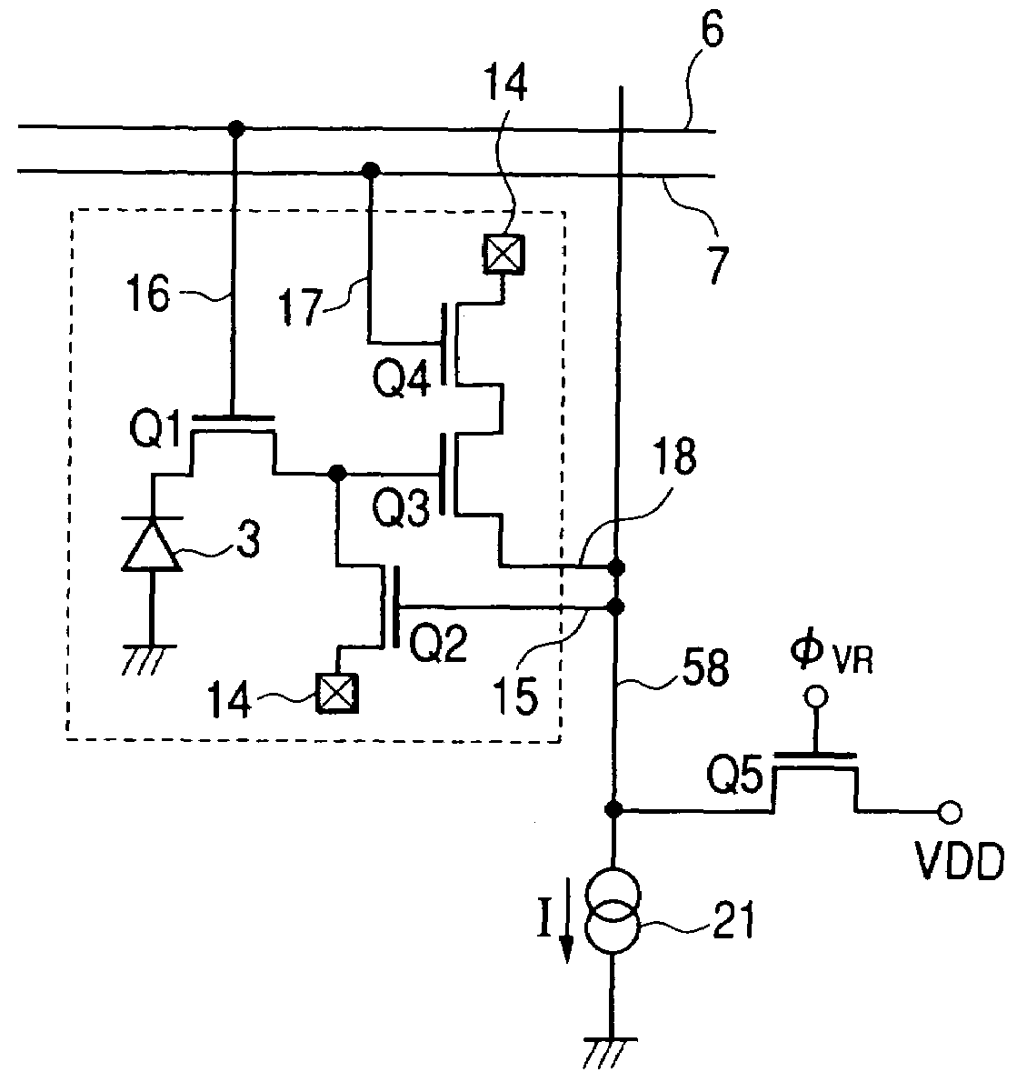
[0077]FIG. 1 is a basic circuit diagram of a unit cell of a solid image pickup device according to this embodiment, and FIG. 2 is a drive timing chart for illustrating a basic operation of the device.

[0078]This embodiment has a signal output line and a reset switch line comprised of (or configured by) one common line as shown by the reference numeral 58.

[0079]A unit cell 1 corresponding to one pixel has at least a photodiode 3 as a photoelectric conversion portion, a transfer switch Q1 as a transfer means, a reset switch Q2 as a reset means, an amplifying means Q3, and a switch Q4 as a selecting means.

[0080]As electrodes and wirings to output optical signals, it has:

[0081]an electrode 17 as well as a selection control line (selecting switch line) 7 to select a unit cell, and

[0082]an electrode 16 as well as transfer control line (transfer switch line) 6 to transfer an electric charge from the photodiode 3 to become a photoelectric conversion portion to an input terminal of an amplify...

embodiment 2

[0102]FIG. 6 is a circuit diagram of two unit cells of the solid image pickup device of this embodiment, FIG. 7 is a drive timing chart thereof, and FIG. 8 is a circuit diagram for 2 rows by 2 columns of a solid image pickup device in which unit cells are arranged in a matrix pattern.

[0103]In this embodiment, one line is multi-used both as a reset switch line for an n-th row and as a selecting switch line for an (n−1)-th row. In FIG. 6, reference numeral 57 denotes a wiring (common line) that are held and used in common between unit cells of two adjoining rows. Reference characters Q1(n), Q2(n), Q3(n), and Q4(n) respectively denote a transfer switch, a reset switch, an amplifying transistor, and a selecting switch of a unit cell of an n-th row while Q1(n−1), Q2(n−1), Q3(n−1), and Q4(n−1) respectively denote a transfer switch, a reset switch, an amplifying transistor, and a selecting switch of a unit cell of (n−1)th row.

[0104]The operation is as follows.

[0105]After the unit cells of ...

embodiment 3

[0114]FIG. 9 is a circuit diagram of two unit cells of the solid image pickup device of this embodiment, FIG. 10 is a drive timing chart thereof, and FIG. 11 is a circuit diagram for 2 rows by 2 columns of a solid image pickup device in which unit cells are arranged in a matrix pattern.

[0115]In this embodiment, a reset switch line for the n-th row and a transfer switch line for the (n−1)-th row are comprised of one common line. In FIGS. 9 and 11, reference numerals 56 denote a wiring (common line) that are held and used in common between two adjoining rows.

[0116]Reference characters Q1(n), Q2(n), Q3(n), and Q4(n) respectively denote a transfer switch, a reset switch, an amplifying transistor, and a selecting switch of a unit cell of an n-th row while Q1(n−1), Q2(n−1), Q3(n−1), and Q4(n−1) respectively denote a transfer switch, a reset switch, an amplifying transistor, and a selecting switch of a unit cell of an (n−1)-th row.

[0117]The operation is as follows.

[0118]After a unit cell o...


PUM


Abstract

A solid image pickup device is disclosed which comprises at least one unit cell having a photoelectric conversion portion, an amplifying means for amplifying a signal generated in the photoelectric conversion portion, a transfer means for transferring the signal to the amplifying means, a reset means for resetting an input terminal of the amplifying means, and a selecting means for selecting the amplifying means and outputting a signal to a signal output line, wherein at least two of a selection control line for controlling the selecting means, a transfer control line for controlling the transfer means, a reset control line for controlling the reset means, and the signal output line in a unit cell, or between two unit cells operating in time series fashion, or between two adjoining unit cells are one common line.

Description

BACKGROUND OF THE INVENTION[0001]1. Field of the Invention[0002]The present invention relates to a solid image pickup device as well as an image pickup system, and in particular relates to a solid image pickup device as well as an image pickup system having signal amplification means per pixel.[0003]2. Related Background Art[0004]As representatives of solid image pickup devices, there is a CCD image sensor comprising photodiodes and CCD shift-registers and an APS (Active Pixel Sensor) comprising photodiodes and MOS transistors.[0005]The APS comprises per pixel a photodiode, a MOS switch, and an amplifying circuit to amplify a signal from the photodiode and has a lot of advantages such that “XY addressing” and “integration of a sensor and a signal processing circuit into one chip” are possible.[0006]Moreover, in recent years, the APS is attracting attention due to improvement in microfabrication technology for MOS transistors and increased requirement for “integration of a sensor and...

Claims


Application Information

Patent Timeline
Patent Type & Authority Patents(United States)
IPC IPC(8): H01L27/00H01L27/146H04N5/374
CPCH01L27/14609H04N5/3741H01L27/14643H04N25/766H04N25/778
Inventor KOIZUMI, TORU
Owner CANON KK
Why Eureka
Try Eureka