High-frequency module and method for manufacturing the same

a technology of high-frequency modules and manufacturing methods, applied in the direction of printed circuit aspects, cross-talk/noise/interference reduction, non-metallic protective coating applications, etc., can solve the problem of difficult to avoid distortion due to baking, and achieve the effect of improving positioning precision and difficult to avoid distortion

Inactive Publication Date: 2006-07-25
PANASONIC SEMICON SOLUTIONS CO LTD
View PDF14 Cites 175 Cited by
  • Summary
  • Abstract
  • Description
  • Claims
  • Application Information

AI Technical Summary

Benefits of technology

[0007]With this high-frequency module, the influence of electromagnetic waves on the high-frequency circuit can be reduced by the metal thin film. Moreover, since the insulating resin supports the metal thin film, the strength or pliability is not a problem as in the case where a thin metal cap is provided, even though the thickness of the metal thin film is reduced. With the insulating resin, it is also possible to reduce the clearance provided below the metal cap. Thus, the height of the high-frequency module can be reduced.
[0009]In the above-mentioned manufacturing method, when a process such as irradiation with a laser beam is performed after the molding of the insulating resin, in order to improve the positioning precision in the process, it is preferable that irradiation with the laser beam or mechanical grinding is performed after positioning based on a mark (e.g., a depression such as a scribe line at which the substrate base material is to be divided into individual substrates, or a portion at which a different type of material such as an electrode for electrical connection to the outside is exposed) that is preformed on an opposed face of a surface of the substrate on which a high-frequency circuit is disposed. This method is effective in particular when a ceramic is used as a substrate material, which makes it difficult to avoid distortions due to baking. In this case, the mark is formed before baking the substrate and the process such as irradiation with the laser beam should be performed while positioning with reference to the mark after baking the substrate.

Problems solved by technology

This method is effective in particular when a ceramic is used as a substrate material, which makes it difficult to avoid distortions due to baking.

Method used


Image

  • High-frequency module and method for manufacturing the same
  • High-frequency module and method for manufacturing the same
  • High-frequency module and method for manufacturing the same

Examples


Embodiment Construction

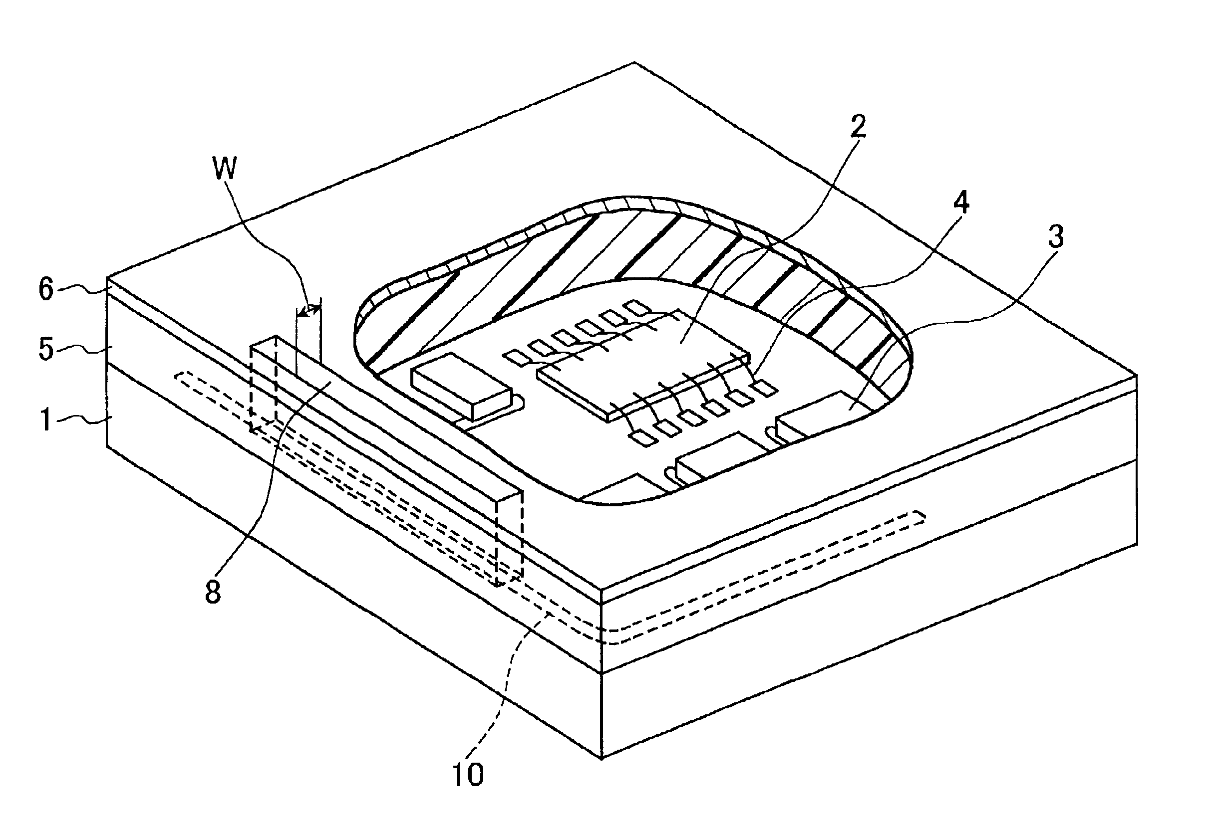
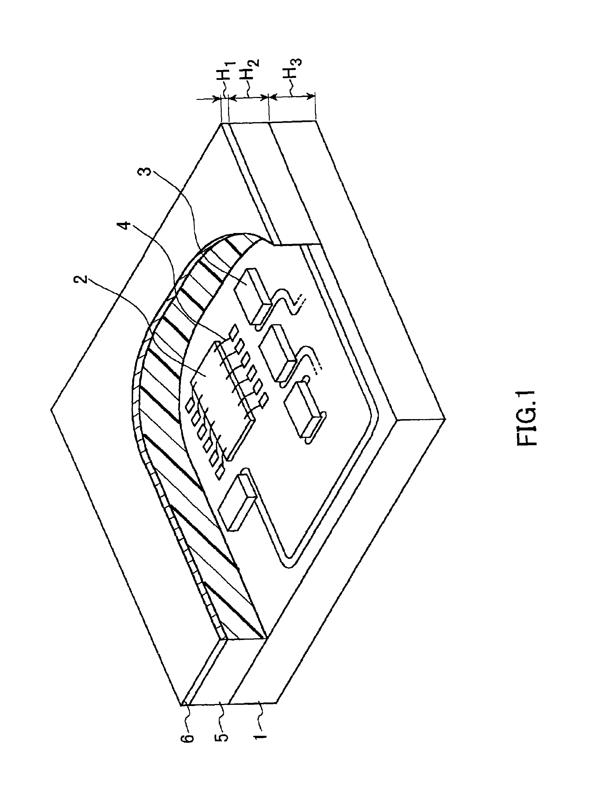
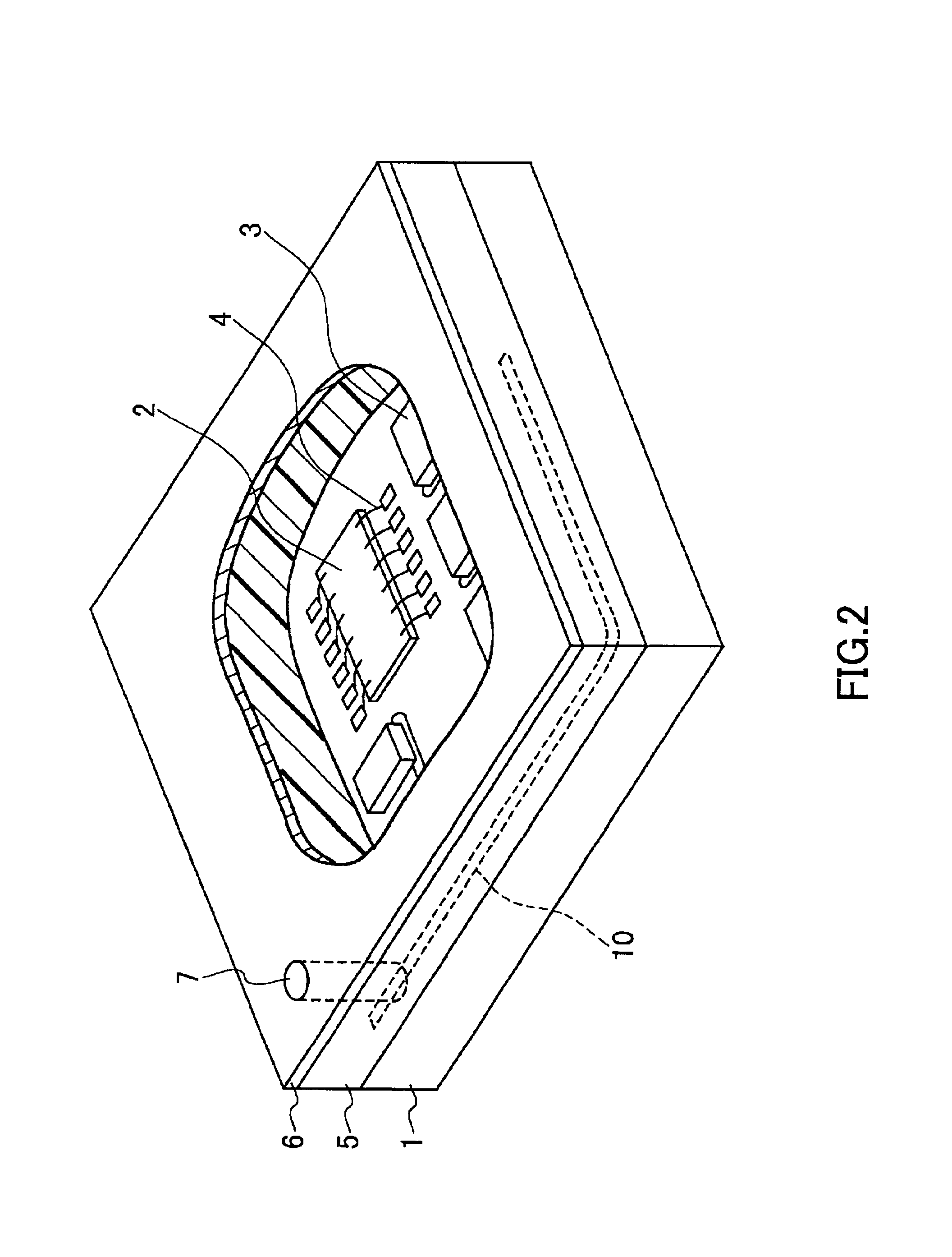
[0022]In the high-frequency module according to the present invention, it is preferable that a wiring pattern that, along with the high-frequency semiconductor element, constitutes a high-frequency circuit on a surface of the substrate is connected electrically to a metal thin film in order to increase the electromagnetic wave shielding effect. More specifically, a first region in which an insulating resin is formed and a second region in which no insulating resin is formed are provided on the aforementioned surface of the substrate, and the wiring pattern exposed at the surface of the substrate in the second region may be connected electrically to the metal thin film.

[0023]When the insulating resin is provided with an aperture so that the wiring pattern is exposed, then it is preferable that the aperture of the insulating resin has a minimum width of at least 0.2 mm and at most 5 mm. If the minimum width is too small, then it becomes difficult to ensure stable electrical contact wi...


PUM


Abstract

In the high-frequency module of the present invention, an insulating resin is formed so as to seal a high-frequency semiconductor element mounted on a surface of a substrate and further to seal electronic components. Furthermore, a metal thin film is formed on the surface of the insulating resin. This metal thin film provides an electromagnetic wave shielding effect.

Description

BACKGROUND OF THE INVENTION[0001]1. Field of the Invention[0002]The present invention relates to a high-frequency module and a method for manufacturing the same.[0003]2. Related Background Art[0004]In high-frequency modules primarily used for mobile communication equipment such as portable telephones, a high-frequency circuit including a high-frequency semiconductor element and a peripheral circuit is formed on a substrate, and a metal cap often is disposed so as to cover a surface of the substrate on which the high-frequency circuit is disposed, in order to protect the high-frequency semiconductor element and shield it from electromagnetic waves. In ordinary conventional high-frequency modules, a high-frequency semiconductor element 102 and electronic components 103 such as chip resistors and chip capacitors are mounted on a substrate 101, and electrically connected to each other by thin metallic wires 104 or a wiring pattern (not shown in detail), thus forming a high-frequency cir...

Claims


Application Information

Patent Timeline
Patent Type & Authority Patents(United States)
IPC IPC(8): H01L31/00H01L23/28H01L23/00H01L23/12H01L23/31H01L23/552H05K1/02H05K3/00H05K3/28H05K9/00
CPCH01L23/3121H01L23/552H01L24/97H05K3/284H01L2924/01023H01L2924/01006H01L2924/01005H01L24/49H01L24/48H05K2201/09918H01L2224/48091H01L2224/48227H01L2224/49175H01L2224/97H01L2924/01004H01L2924/01013H01L2924/01029H01L2924/01033H01L2924/01039H01L2924/01047H01L2924/01074H01L2924/01078H01L2924/01079H01L2924/01082H01L2924/16152H01L2924/19041H01L2924/19043H01L2924/19105H01L2924/3025H05K1/0218H05K3/0052H01L2224/85H01L2924/00014H01L2924/00H01L24/45H01L2224/451H01L2924/12042H01L2924/15159H01L2924/15787H01L2924/16195H01L2924/181H01L2924/1815H01L2924/00015H01L2224/05599H01L2924/00012H01L23/00H05K9/00
Inventor TAKEHARA, HIDEKIYOSHIKAWA, NORIYUKIKANAZAWA, KUNIHIKO
Owner PANASONIC SEMICON SOLUTIONS CO LTD
Why Eureka
Try Eureka