Method and device for detecting and processing electric and optical signals

a technology of optical signals and methods, applied in the field of optoelectronics, can solve the problems of inability to use known methods, inflexible pmd and methods used therewith, and inability to select time, and achieve the effect of extreme amplification effects

Inactive Publication Date: 2006-07-25
PMDTECHNOLOGIES
View PDF4 Cites 8 Cited by
  • Summary
  • Abstract
  • Description
  • Claims
  • Application Information

AI Technical Summary

Benefits of technology

[0009]The impressive success with and great advantages of optical information processing could be substantially better used and enlarged by a suitable versatile and intelligent method of optoelectronic detection, processing and transmission with new options in terms of direct inherent digital and analog signal processing of the incoming optical signal wave with electrical signals or other optical signals, which in addition can be inexpensively carried out in microelectronically and microoptically integrated fashion in the form of OE interface components or OE processor components respectively.
[0110]The sought combination of spectral line and relaxation time τ=φ / ω, with the OEP array, permits great advances in fast and precise substance analysis, in particular in time-resolved spectral analysis.

Problems solved by technology

The known PMD and the methods used therewith are however relatively inflexible and have no time selection, no inherently switchable zero condition of the output signal and no analog or digital interlinking of a plurality of electrical and optical input signals.
In particular it is not possible with that known method and the known PMD to mix and link together different optical signals.

Method used


Image

  • Method and device for detecting and processing electric and optical signals
  • Method and device for detecting and processing electric and optical signals
  • Method and device for detecting and processing electric and optical signals

Examples


Embodiment Construction

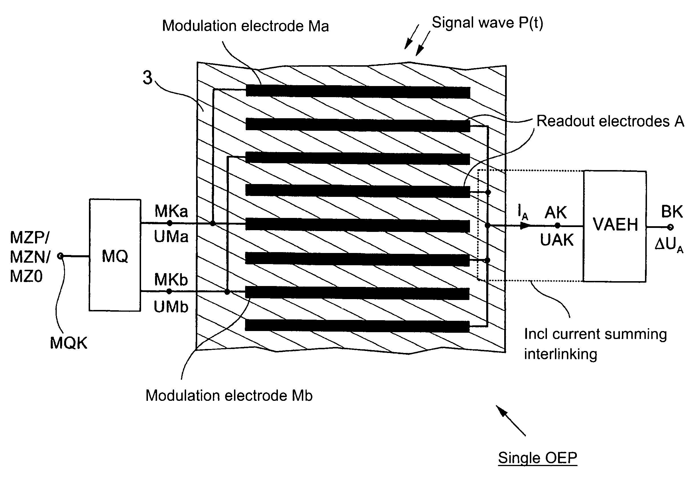
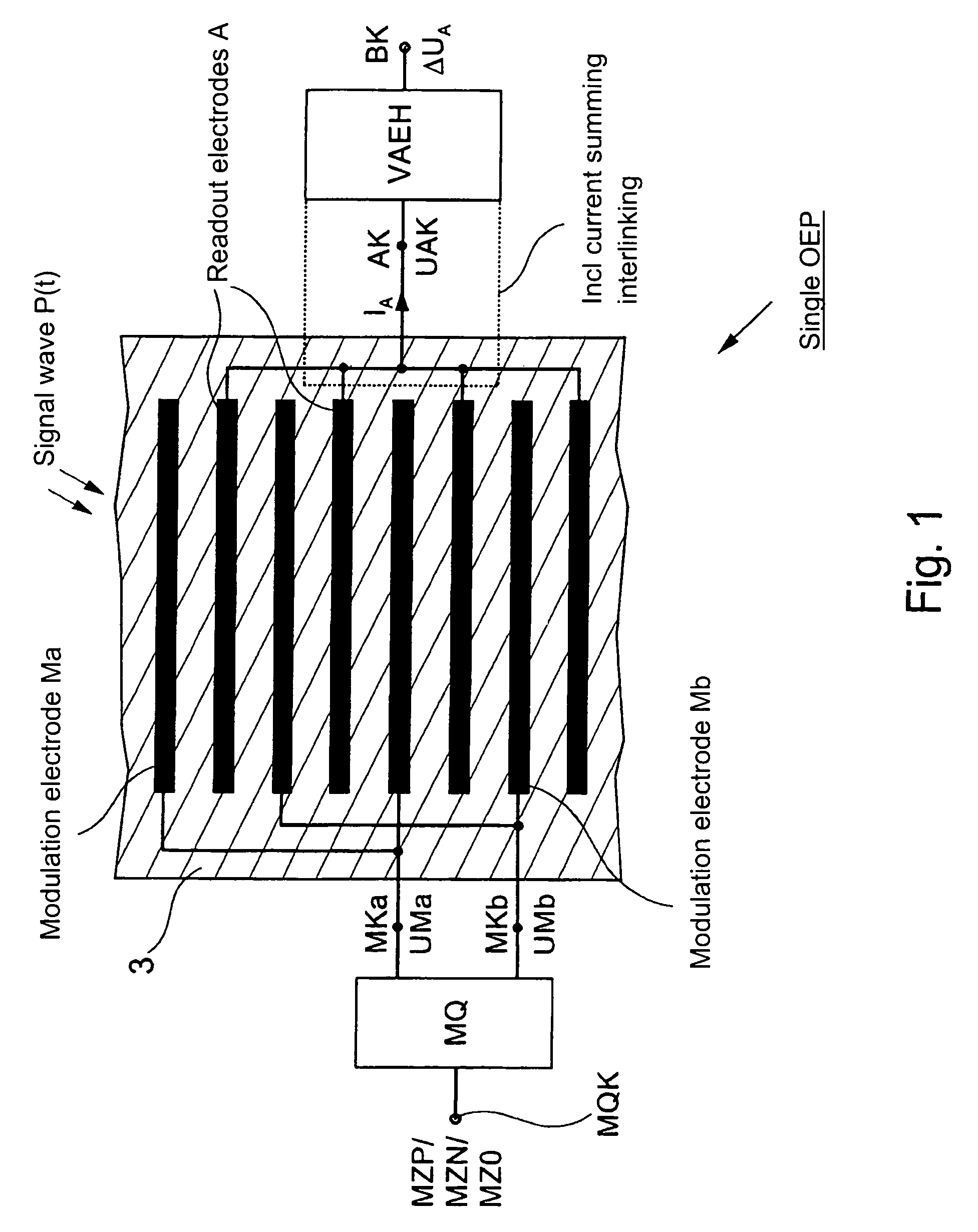
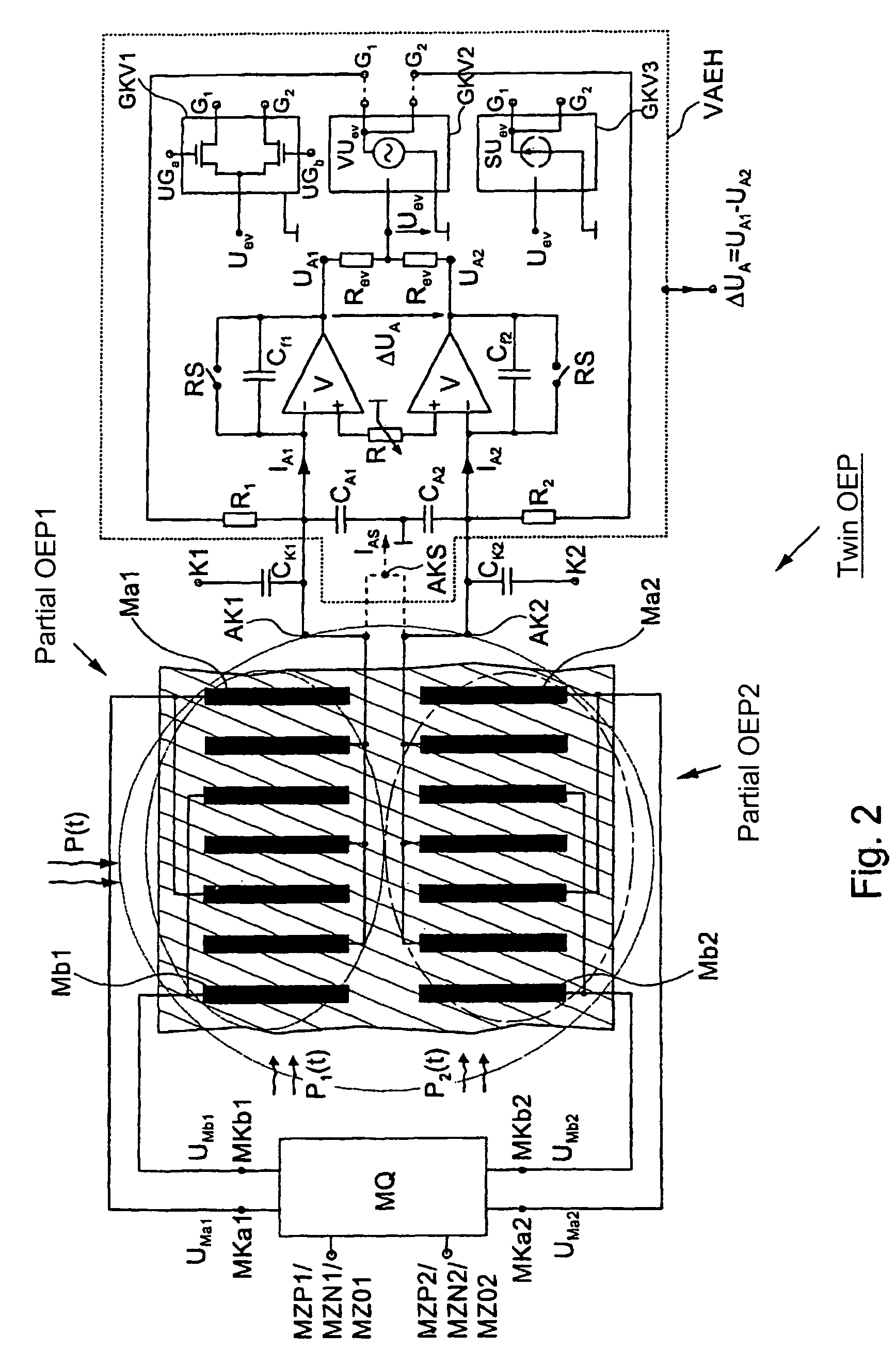
[0120]FIG. 1 shows the surface of an article 3 which is sensitive to signal waves, with a regular covering of similar modulation electrodes Ma and Mb, between each of which are disposed the respective readout electrodes A. A signal wave P(t) which is distributed as equally as possible generates charge carriers in the modulation and readout region, identified in that way, between the electrodes. The modulation electrodes are modulated by the modulation source MQ at the terminals MKa and MKb with the associated modulation voltages UMa and UMb and thus influence distribution and the direction of the read-out charge carrier current IA at the readout terminal AK. The readout potential UAK is preferably selected to be zero or earth potential by means of a low-ohmic readout unit VAEH. Clearly defined modulation conditions which can be predetermined by way of the input terminal MQK of the modulation source MQ are firstly the condition, identified by MZP, with maximum positive current condit...


PUM


Abstract

A method for detecting and / or processing signal waves that produce charge carriers in an article sensitive to the signal waves. At least two modulation electrodes are provided, at least one of which is disposed in proximity to a readout-electrode in such a manner that, depending on the polarity sign of the modulation voltage of the modulation electrode, the current flowing across the readout electrode is positive or negative. The invention further relates to a device for detecting and processing signal waves. The invention provides a method and a device that is capable of interlinking various optical and / or electronic signals in a logically digital or analogous manner or to detect the course of optical signals by scanning (time interval measurements).

Description

BACKGROUND OF THE INVENTION[0001]1. Field of the Invention[0002]The present invention relates generally to optoelectronics and more specifically to methods and apparatus for detecting and processing electrical and optical signals.[0003]2. Discussion of Related Art[0004]Corresponding methods and apparatuses are known for example as “PMD elements” from German patent application No 196 35 932.5 or corresponding international patent application WO 98 / 10255 and DE 198 21 974.1 and corresponding international patent application WO 99 / 60629.[0005]The state of the art in regard to that inherent pre-processing of optical signal waves is described for example in “Handbook of Computer Vision and Applications”, Volume 1, Sensors and Imaging, edited by Jähne et al., Academic Press, on pages 463ff and also in dozens of publications relating to uses as laser radar, 3D cameras and OE interfaces for communication, for example on the homepage of the Institut für Nachrichtenverarbeitung of the Univers...

Claims


Application Information

Patent Timeline
Patent Type & Authority Patents(United States)
IPC IPC(8): G02B26/00G01J3/433H01L27/14H03D9/06
CPCH03D9/0608G01J9/00
Inventor SCHWARTE, RUDOLF
Owner PMDTECHNOLOGIES
Why Eureka
Try Eureka