Method, system and medium for process control for the matching of tools, chambers and/or other semiconductor-related entities

a technology of process control and matching, applied in the field of process control for matching, can solve the problems of not having a method or process to provide automatic communication of modification, each component of an assembly line, module, is adjusted separately, etc., and achieves the effect of improving the consistency of the results of a given recipe and a better form of control

Inactive Publication Date: 2006-07-25
APPLIED MATERIALS INC
View PDF403 Cites 88 Cited by
  • Summary
  • Abstract
  • Description
  • Claims
  • Application Information

AI Technical Summary

Benefits of technology

[0011]The present invention addresses the deficiencies of the conventional technology described above by, e.g., capturing behaviors of one or more assembly line components, and communicating those behaviors to appropriate components of, e.g., other assembly lines within a foundry to, e.g., improve the consistency of the results of a given recipe(s) from use to use. Th...

Problems solved by technology

However, if one were to contemplate conveying those modification settings to, e.g., other tools on another assembly line making the same product, a problem one would encounter is that each component of an assembly line, e.g., chambers, tools and modules, is adjusted separately and independently, even though the same product is being fabricated in parallel on another assembly line.
While modifications made to one tool or chamber on, e.g., one assembly line cou...

Method used


Image

  • Method, system and medium for process control for the matching of tools, chambers and/or other semiconductor-related entities
  • Method, system and medium for process control for the matching of tools, chambers and/or other semiconductor-related entities
  • Method, system and medium for process control for the matching of tools, chambers and/or other semiconductor-related entities

Examples


Embodiment Construction

[0044]The following detailed description includes many specific details. The inclusion of such details is for the purpose of illustration only and should not be understood to limit the invention. Throughout this discussion, similar elements are referred to by similar numbers in the various figures for ease of reference. In addition, features in one embodiment may be combined with features in other embodiments of the invention.

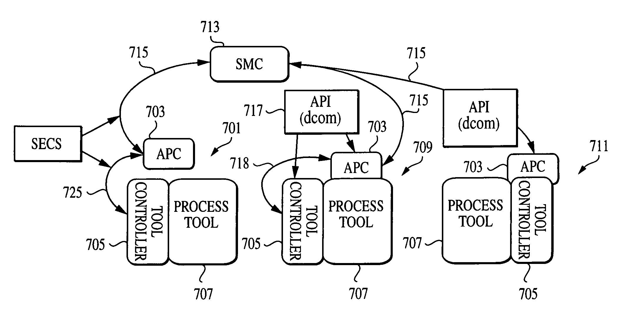
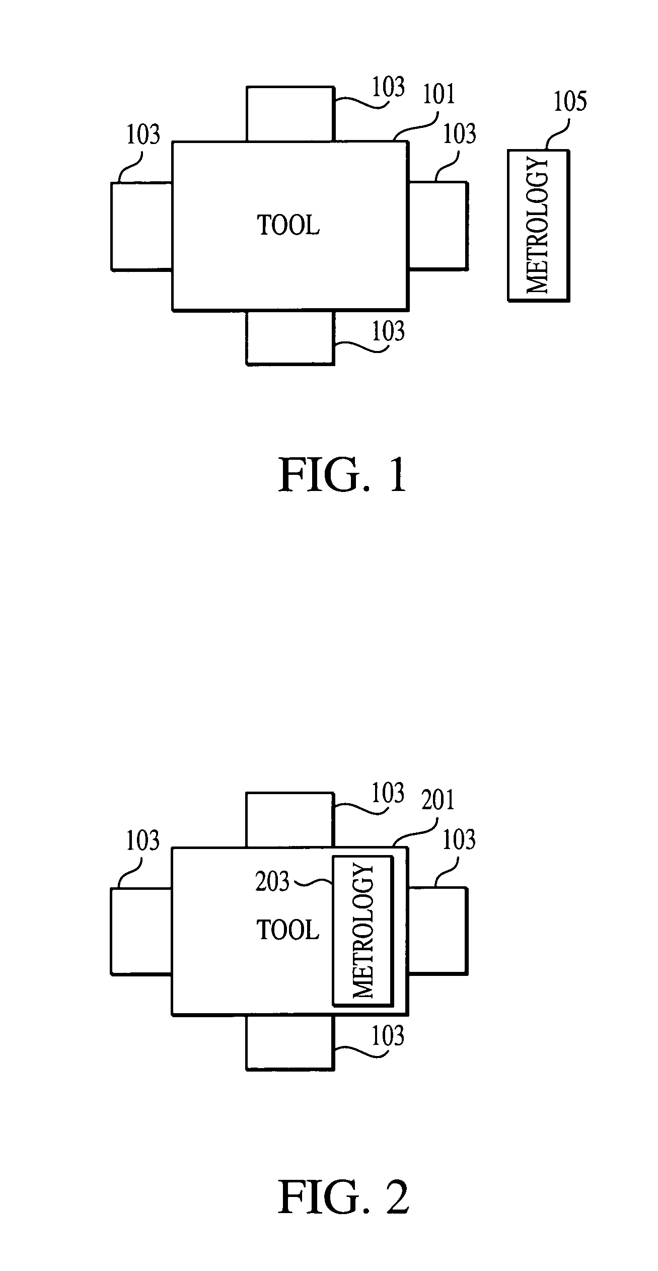
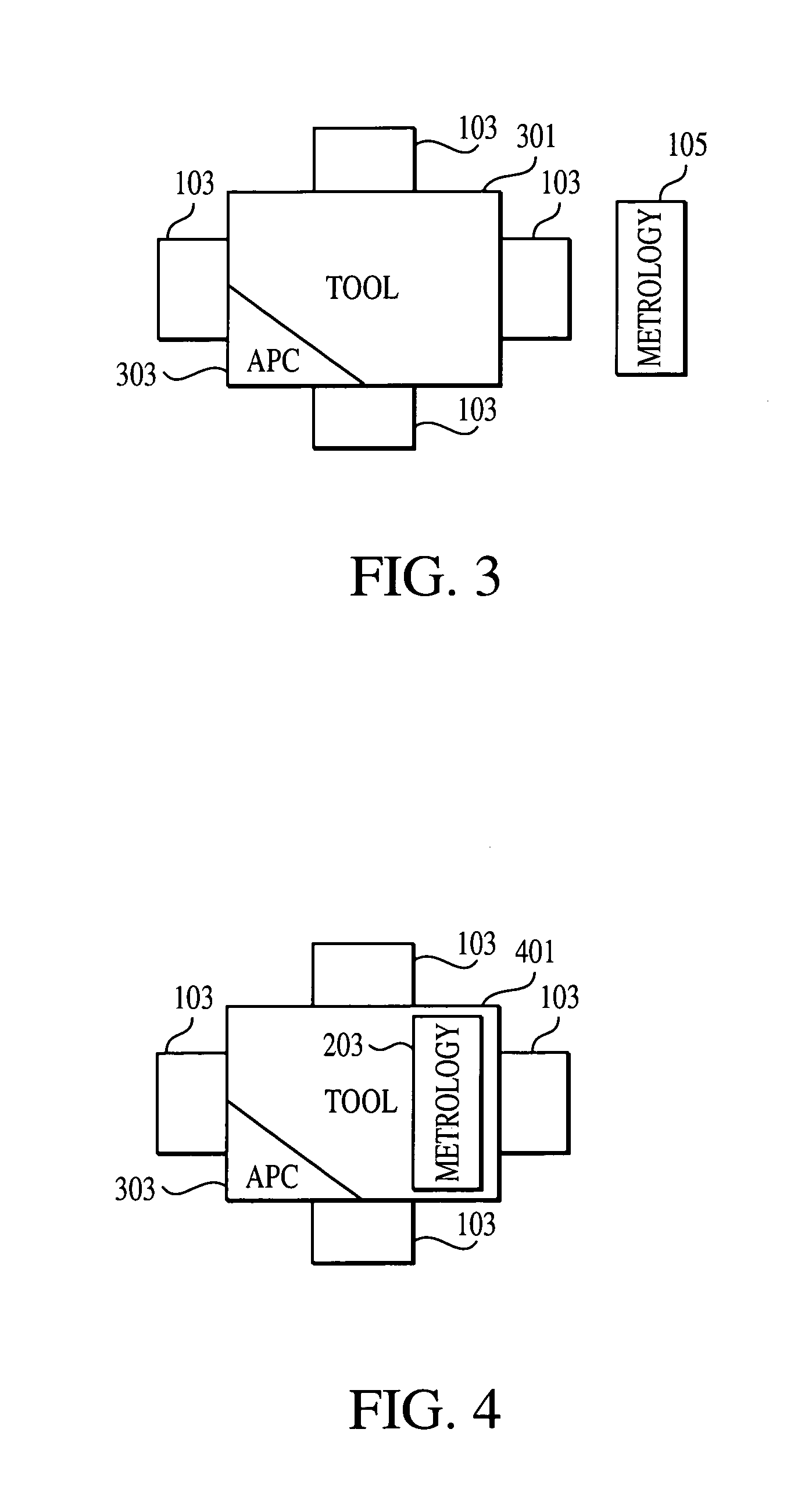
[0045]A process control system, such as a semi-conductor fabrication plant, may include process tools each perhaps with multiple chambers, wherein each of the chambers is intended to work in parallel on a stream of products, to produce essentially identical products or products where at least some of the processing is essentially identical. One or more embodiments of the present invention concern matching (e.g., imparting the behavior information of one component to another component) between one or more comparably configured components (e.g., chambers on one o...


PUM


Abstract

The invention relates to a method, system and computer program useful for producing a product, such as a microelectronic device, for example in an assembly line, where the production facility includes parallel production of assembly lines of products on identically configured chambers, tools and/or modules. Control is provided between such chambers. Behaviors of a batch of wafers (or of each wafer) are collected as the first batch (or each wafer) is processed by one of the identically configured chambers in one assembly line to produce the microelectronic device. The information relating to the behavior is shared with a controller of another one (or more) of the identically configured chambers, process tools and/or modules, to provide an adjustment of the process tool and thereby to produce a second batch (or next wafer) which is substantially identical, within tolerance, to the first batch (or wafer).

Description

CROSS REFERENCES TO RELATED APPLICATIONS[0001]This application claims the benefit of U.S. Provisional Application Ser. No. 60 / 365,782 filed Mar. 21, 2002, expressly incorporated herein by reference; and U.S. Provisional Application Ser. No. 60 / 298,878 filed Jun. 19, 2001, expressly incorporated herein by reference.BACKGROUND OF THE INVENTION[0002]1. Field of the Invention[0003]The present invention concerns computer-implemented and / or computer assisted methods, systems and mediums for enabling improved control (e.g., parallel control) during advanced process control. More specifically, one or more embodiments of the present invention relate to enhanced control of the processing of products, such as semi-conductor wafers, on comparably configured processing devices, such as chambers, utilizing behavior information.[0004]2. Related Art[0005]Microelectronic products, such as semi-conductor chips, are fabricated in foundries. In a foundry, batches of products are typically fabricated in...

Claims


Application Information

Patent Timeline
IPC IPC(8): G06F19/00G05B13/02B24B37/04B24B49/03B24B49/18B24B53/007G05B19/00G05B19/19G05B19/418H01L21/00H01L21/3105H01L21/66
CPCB24B37/042B24B49/03B24B49/18B24B53/017G05B19/00G05B19/19H01L22/20H01L21/67276G05B19/41865G05B2219/32053G05B2219/32065G05B2219/45031H01L21/31053H01L21/67253Y02P90/02
Inventor SHANMUGASUNDRAM, ARULKUMAR P.ARMER, HELENSCHWARM, ALEXANDER T.
Owner APPLIED MATERIALS INC
Why Eureka
Try Eureka