Semiconductor devices having a hybrid channel layer, current aperture transistors and methods of fabricating same

a technology of current aperture transistor and hybrid channel layer, which is applied in the direction of semiconductor devices, radio frequency controlled devices, electrical apparatus, etc., can solve the problems of less breakdown voltage, limiting the potential applications of the device, and breakdown occurring in the region of field crowding rather than in the bulk material. , to achieve the effect of higher doping level

Active Publication Date: 2006-08-01
CREE INC
View PDF100 Cites 108 Cited by
  • Summary
  • Abstract
  • Description
  • Claims
  • Application Information

AI Technical Summary

Problems solved by technology

For example, the maximum reverse bias blocking voltage sustainable by the device may limit the potential applications for the device.
In conventional transistors, the structure of the device may result in a breakdown voltage that is less than the breakdown voltage of the device.
For example, in a conventional U-metal oxide semiconductor field effect transistor (UMOSFET), field crowding may result at a corner of the gate trench such that breakdown occurs in the region of the field crowding rather than in the bulk material.

Method used


Image

  • Semiconductor devices having a hybrid channel layer, current aperture transistors and methods of fabricating same
  • Semiconductor devices having a hybrid channel layer, current aperture transistors and methods of fabricating same
  • Semiconductor devices having a hybrid channel layer, current aperture transistors and methods of fabricating same

Examples


Embodiment Construction

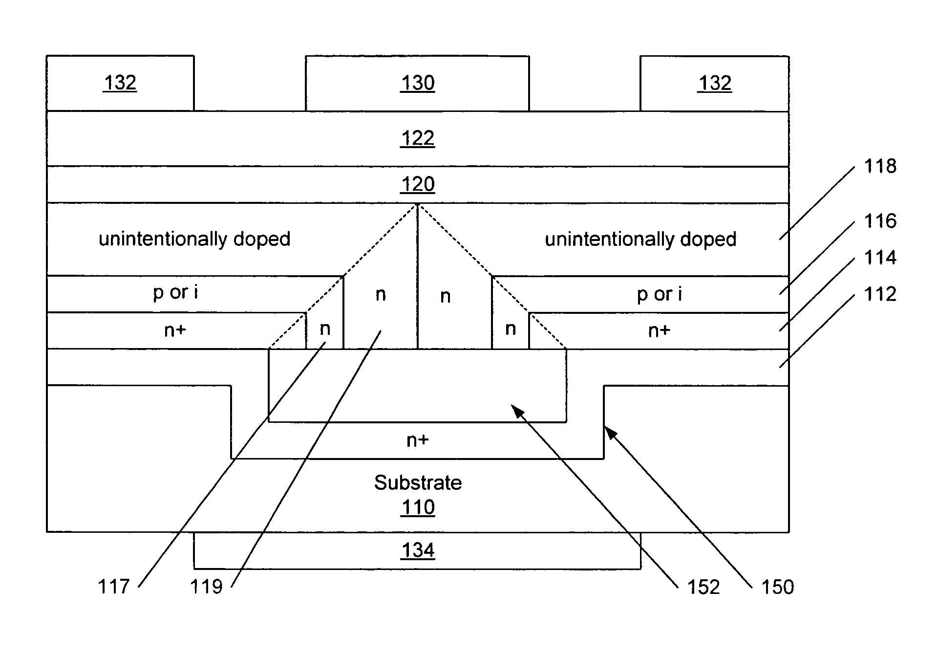
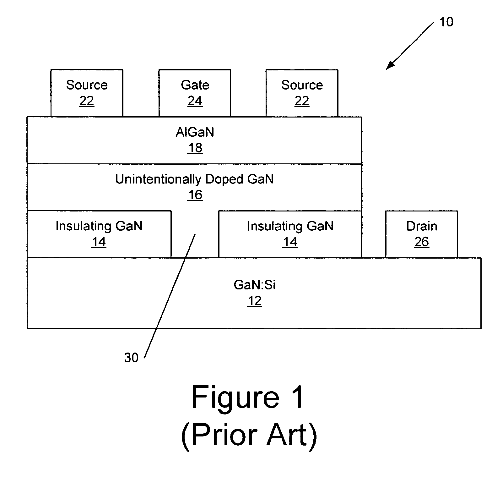
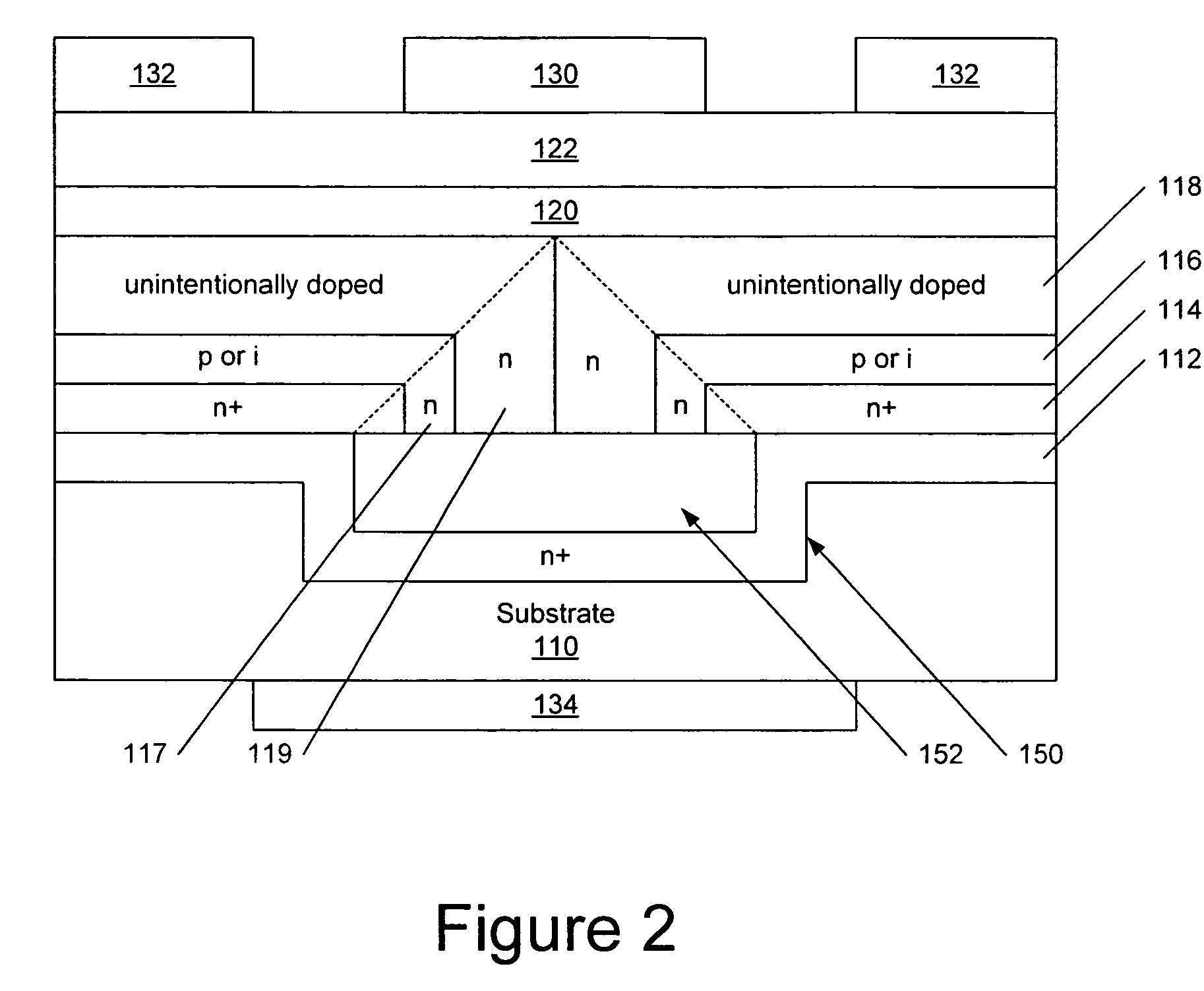
[0028]The present invention now will be described more fully hereinafter with reference to the accompanying drawings, in which embodiments of the invention are shown. This invention may, however, be embodied in many different forms and should not be construed as limited to the embodiments set forth herein. Rather, these embodiments are provided so that this disclosure will be thorough and complete, and will fully convey the scope of the invention to those skilled in the art. In the drawings, the size and relative sizes of layers and regions may be exaggerated for clarity. It will be understood that when an element or layer is referred to as being “on”, “connected to” or “coupled to” another element or layer, it can be directly on, connected or coupled to the other element or layer or intervening elements or layers may be present. In contrast, when an element is referred to as being “directly on,”“directly connected to” or “directly coupled to” another element or layer, there are no ...


PUM


Abstract

Transistors and / or methods of fabricating transistors that include a source contact, drain contact and gate contact are provided. In some embodiments, a channel region is provided between the source and drain contacts and at least a portion of the channel regions includes a hybrid layer comprising semiconductor material. In particular embodiments of the present invention, the transistor is a current aperture transistor. The channel region may include pendeo-epitaxial layers or epitaxial laterally overgrown layers. Transistors and methods of fabricating current aperture transistors that include a trench that extends through the channel and barrier layers and includes semiconductor material therein are also provided.

Description

FIELD OF THE INVENTION[0001]The present invention relates to semiconductor devices and, more particularly, to current aperture transistors.BACKGROUND[0002]In high voltage / high power electronic devices, a performance characteristic of importance may be the breakdown characteristics of the device. For example, the maximum reverse bias blocking voltage sustainable by the device may limit the potential applications for the device. In conventional transistors, the structure of the device may result in a breakdown voltage that is less than the breakdown voltage of the device. For example, in a conventional U-metal oxide semiconductor field effect transistor (UMOSFET), field crowding may result at a corner of the gate trench such that breakdown occurs in the region of the field crowding rather than in the bulk material. Various structures have been proposed in different types of transistors to provide breakdown voltages of the transistors that approach the bulk breakdown voltage of the mat...

Claims


Application Information

Patent Timeline
Patent Type & Authority Patents(United States)
IPC IPC(8): H01L29/768H01L21/00H01L21/335H01L29/10H01L29/20H01L29/778H01L31/072
CPCH01L29/0649H01L29/0657H01L29/1029H01L29/7788H01L29/66462H01L29/7783H01L29/7787H01L29/2003
Inventor SAXLER, ADAM WILLIAM
Owner CREE INC
Why Eureka
Try Eureka