Semiconductor memory cell, array, architecture and device, and method of operating same

a memory cell and semiconductor technology, applied in the field of semiconductor memory cells, arrays, architecture and devices, can solve the problems of complex and expensive integration of one transistor-one capacitor memory cells into logic devices, the source or drain regions of non-symmetrical devices are typically not interchangeable, and the device size is limited or restricted

Inactive Publication Date: 2006-08-01
MICRON TECH INC
View PDF245 Cites 243 Cited by
  • Summary
  • Abstract
  • Description
  • Claims
  • Application Information

AI Technical Summary

Problems solved by technology

Although significant integration densities can be achieved with DRAM devices employing one transistor-one capacitor memory cells, such devices tend to be limited or restricted with respect to the size of the memory cell.
As a result, integration of one transistor-one capacitor memory cells into logic devices is often complicated and expensive.
As such, the source or drain regions of a non-symmetrical device are typically not interchangeable.

Method used


Image

  • Semiconductor memory cell, array, architecture and device, and method of operating same
  • Semiconductor memory cell, array, architecture and device, and method of operating same
  • Semiconductor memory cell, array, architecture and device, and method of operating same

Examples


Embodiment Construction

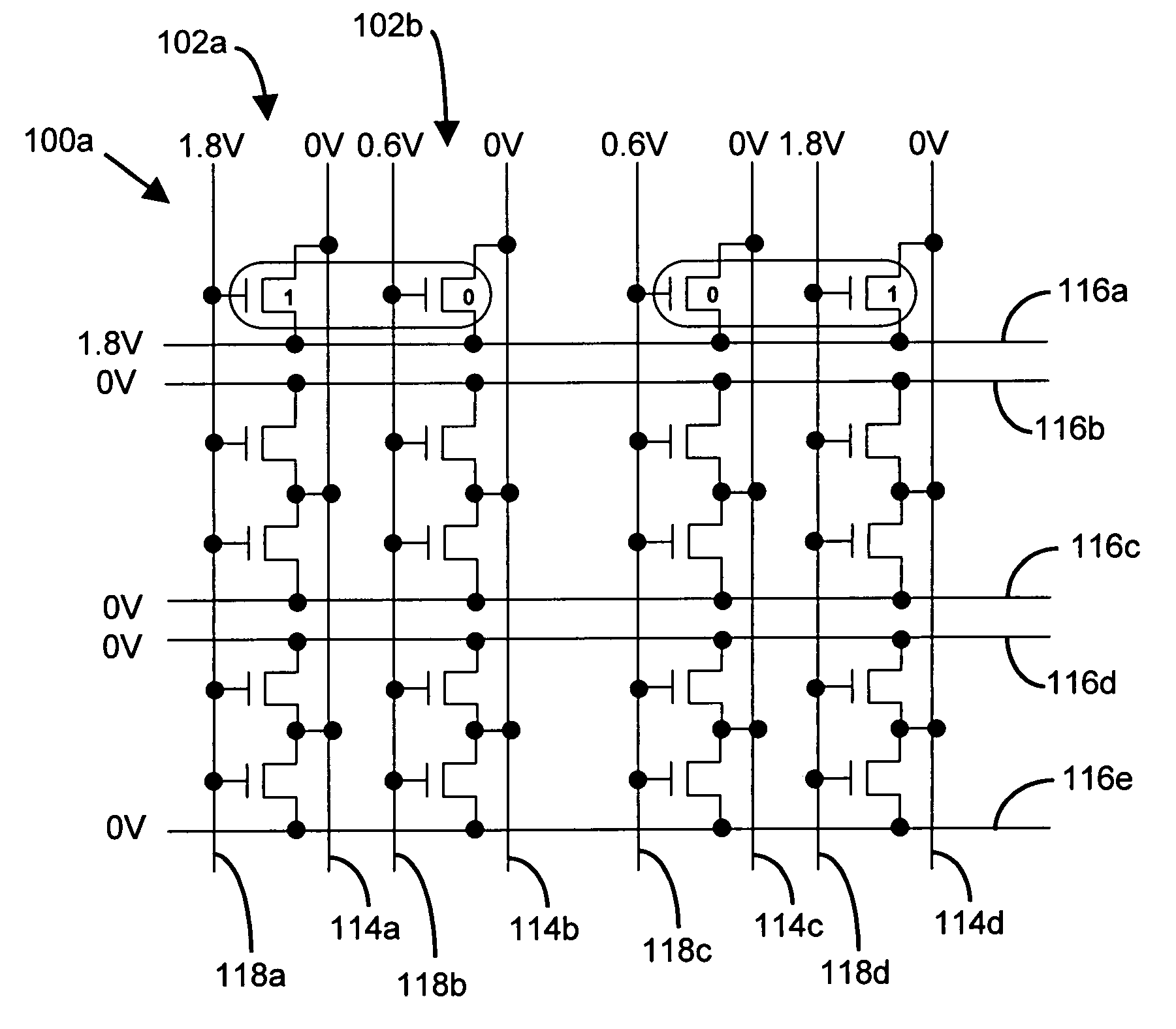
[0054]There are many inventions described and illustrated herein. In a first aspect, the present invention is directed to a memory cell and technique of reading data from and writing data into that memory cell. In this regard, in one embodiment of this aspect of the invention, the memory cell includes two transistors which store complementary data states. That is, the two-transistor memory cell includes a first transistor that maintains a complementary state relative to the second transistor. As such, when programmed, one of the transistors of the memory cell stores a logic low (a binary “0”) and the other transistor of the memory cell stores a logic high (a binary “1”).

[0055]The data state of the two-transistor complementary memory cell may be read and / or determined by sampling, sensing measuring and / or detecting the polarity of the logic states stored in each transistor of complementary memory cell. That is, the two-transistor complementary memory cell is read by sampling, sensing...


PUM


Abstract

There are many inventions described and illustrated herein. In a first aspect, the present invention is directed to a memory cell and technique of reading data from and writing data into that memory cell. In this regard, in one embodiment of this aspect of the invention, the memory cell includes two transistors which store complementary data states. That is, the two-transistor memory cell includes a first transistor that maintains a complementary state relative to the second transistor. As such, when programmed, one of the transistors of the memory cell stores a logic low (a binary “0”) and the other transistor of the memory cell stores a logic high (a binary “1”). The data state of the two-transistor complementary memory cell may be read and / or determined by sampling, sensing measuring and / or detecting the polarity of the logic states stored in each transistor of complementary memory cell. That is, the two-transistor complementary memory cell is read by sampling, sensing measuring and / or detecting the difference in signals (current or voltage) stored in the two transistors.

Description

CROSS-REFERENCE TO RELATED APPLICATIONS[0001]This application claims priority to: U.S. Provisional Application Ser. No. 60 / 470,385, entitled “Two Transistor Gain Cell”, filed May 13, 2003 (hereinafter “the Provisional Application”). The contents of the Provisional Application are incorporated by reference herein in their entirety.BACKGROUND[0002]This invention relates to a semiconductor memory cell, array, architecture and device, and techniques for controlling and / or operating such cell and device; and more particularly, in one aspect, to a semiconductor dynamic random access memory (“DRAM”) cell, array, architecture and / or device wherein the memory cell includes an electrically floating body in which an electrical charge is stored.[0003]There are many different types and / or forms of DRAM cells, including, for example, a semiconductor memory cell consisting of an access transistor and a capacitor, which stores an electric charge representing a bi-stable memory state. The access tra...

Claims


Application Information

Patent Timeline
Patent Type & Authority Patents(United States)
IPC IPC(8): G11C11/24G11C11/404G11C16/04G11C16/28H01LH01L27/108
CPCG11C11/404G11C16/28H01L29/7841H01L27/108H01L27/10802G11C2211/4013G11C2211/4016H10B12/20H10B12/00
Inventor FERRANT, RICHARDOKHONIN, SERGUEICARMAN, ERICBRON, MICHEL
Owner MICRON TECH INC
Why Eureka
Try Eureka