Laminated structure, method of manufacturing the same and ultrasonic transducer array

a technology of ultrasonic transducer array and laminate structure, which is applied in the direction of mechanical vibration separation, piezoelectric/electrostrictive/magnetostrictive device details, semiconductor/solid-state device details, etc., can solve the problems of reducing the performance of piezoelectric actuator, and reducing the efficiency of piezoelectric actuator

Inactive Publication Date: 2006-08-08
FUJIFILM HLDG CORP +1
View PDF8 Cites 22 Cited by
  • Summary
  • Abstract
  • Description
  • Claims
  • Application Information

AI Technical Summary

Benefits of technology

[0009]The present invention has been achieved in view of the above-described problems. A first object of the present invention is to provide a laminated structure with less breakage of insulative layers due to stress. Further, a second object of the present invention is to provide a manufacturing method of laminated structure by which such a laminated structure can be easily manufactured. Furthermore, a third object of the present invention is to provide an ultrasonic transducer array using such a laminated structure.
[0014]According to the present invention, an electrode layer is formed by employing two kinds of materials and an electrode is insulated from one side electrode by oxidizing or fluorinating an end surface of one of those materials, and therefore, a region of a piezoelectric material layer on which the electrode is not disposed can be reduced to the minimum. As a result, a laminated structure with less breakage of the insulative layer due to stress can be fabricated easily.

Problems solved by technology

In the microfabrication of an element having opposed electrodes, the smaller the area of the element is made, the smaller the capacitance between the electrodes becomes, so that a problem of rise in the electric impedance of the element occurs.
On this account, when the electric impedance rises in a piezoelectric actuator, for example, the impedance matching between the piezoelectric actuator and a signal circuit for driving the piezoelectric actuator cannot be established, and it becomes difficult to feed power to the piezoelectric actuator, and thereby, the performance of the piezoelectric actuator is degraded.
On this account, a problem that stress is concentrated on this part and the part is easy to break occurs.
However, forming interconnection to each of the large number of laminated structures in accordance with such method is complicated, and especially, in the case where the laminated structure is arrayed in a two-dimensional manner, the interconnection is difficult to be formed.

Method used


Image

  • Laminated structure, method of manufacturing the same and ultrasonic transducer array
  • Laminated structure, method of manufacturing the same and ultrasonic transducer array
  • Laminated structure, method of manufacturing the same and ultrasonic transducer array

Examples


first embodiment

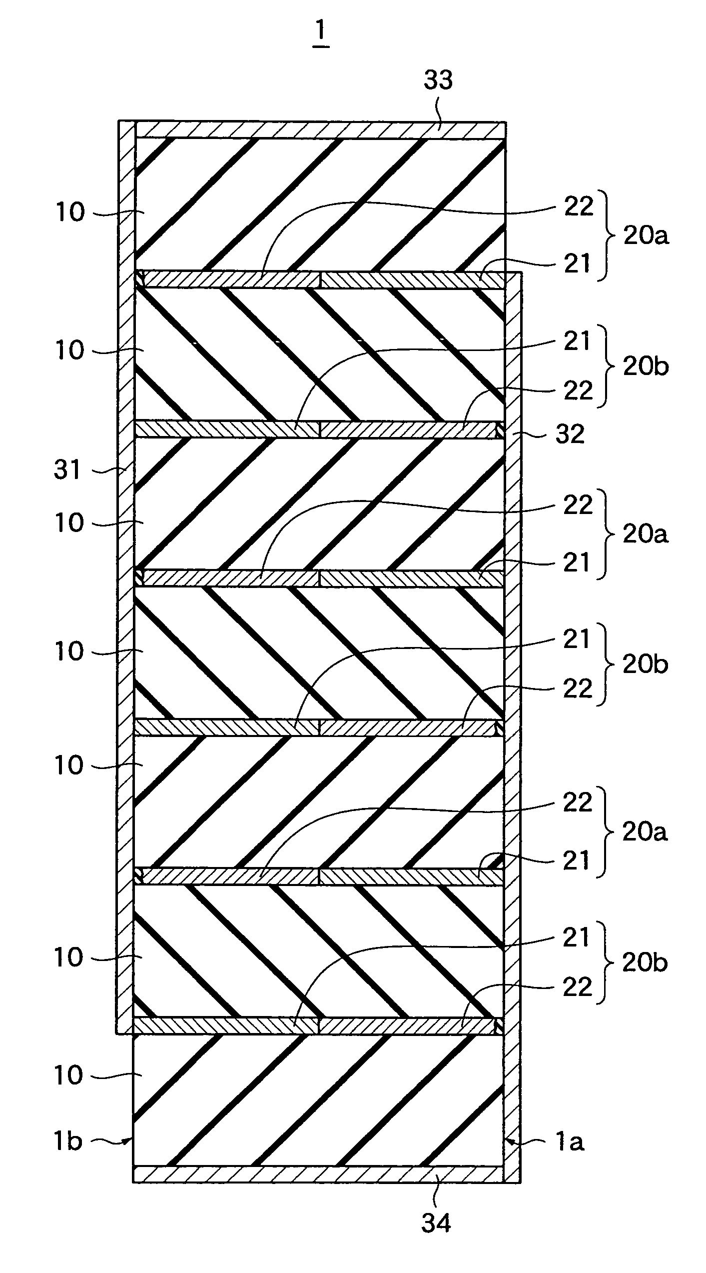
[0025]FIG. 1 is a sectional view showing a laminated structure according to the present invention. The laminated structure 1 is a micro columnar structural body having a bottom surface with sides on the order of 0.2 mm to 1.0 mm and a height on the order of 1.0 mm. In this embodiment, a piezoelectric material is used as a dielectric. The laminated structure 1 includes a plurality of piezoelectric material layers 10, a plurality of electrode layers 20a and 20b containing two kinds of electrode materials, side electrodes 31 and 32 formed on side surfaces 1a and 1b of the laminated structure 1, respectively. Further, the laminated structure 1 may include an upper electrode 33 and a lower electrode 34 connected to the side electrodes 31 and 32, respectively. The shape of the bottom surface of the laminated structure 1 is not limited to a square shape, but may be a rectangular shape or other shapes. Further, the regions in which side electrodes are disposed are not limited to a pair of o...

third embodiment

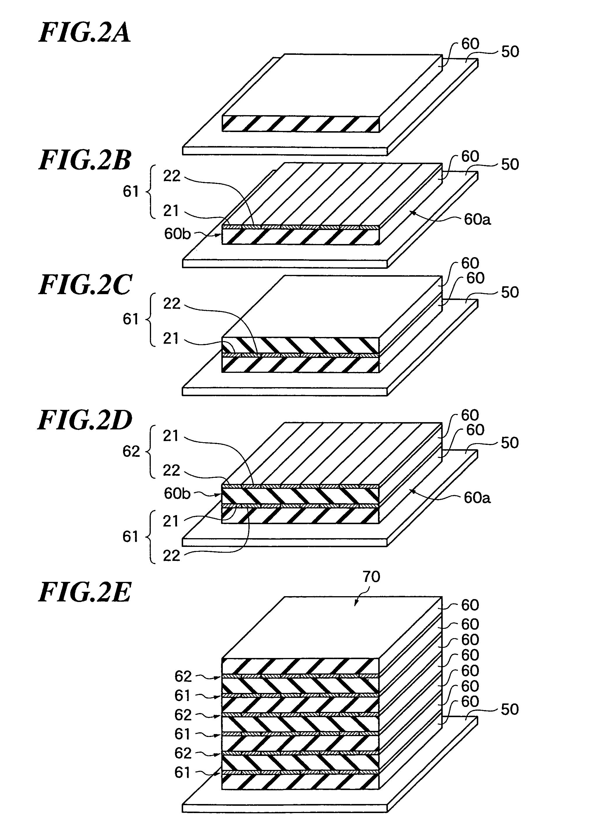
[0058]As described above, according to the manufacturing method of laminated structure when internal electrodes of the laminated structure 73 are formed by two kinds of materials, one laminated structure is fabricated by arranging the respective electrode materials so as to have widths substantially equal to the width of one laminated structure, and, after formation of the laminated structure 73, cutting the nearly center portions of the electrode materials. Therefore, in the case where the electrodes are formed by employing two kinds of materials, positional accuracy of the positional relationship between the different electrode layers can be relaxed, and the two kinds of electrode materials can be reliably exposed in the side surfaces in precise positional relationship in the respective laminated structures after being cut. Further, in the case where the laminated structure 73 is cut in accordance with the sand blast method using a mask, laminated structures having desired shapes...


PUM

PropertyMeasurementUnit
heightaaaaaaaaaa
heightaaaaaaaaaa
velocityaaaaaaaaaa

Abstract

A laminated structure with less breakage of an insulative layer due to stress and easy interconnection. The laminated structure includes at least a first electrode layer, a dielectric layer and a second electrode layer stacked in this order. The first electrode layer includes a first electrode material disposed such that an end surface thereof is exposed in a first side region of the laminated structure and a second electrode material having an insulating film formed on an end surface in a second side region of the laminated structure. The second electrode layer includes the first electrode material disposed such that an end surface is exposed in the second side region of the laminated structure and the second electrode material having an insulating film formed on an end surface in the first side region of the laminated structure.

Description

BACKGROUND OF THE INVENTION[0001]1. Field of the Invention[0002]The present invention relates to a laminated structure in which insulator layers and electrode layers are alternately stacked, and a method of manufacturing the laminated structure. Further, the present invention relates to an ultrasonic transducer array including a plurality of such laminated structures, to be used for ultrasonic diagnosis, nondestructive inspection and so on.[0003]2. Description of a Related Art[0004]Laminated structures in each of which insulator (dielectric) layers and electrode layers are alternately formed, are utilized, not only in laminated capacitors, but also in various other uses such as piezoelectric pumps, piezoelectric actuators and ultrasonic transducers. In recent years, with the developments of devices and equipment concerning MEMS (micro electromechanical systems), elements each having such a laminated structure have been microfabricated still further and packaged more highly.[0005]In ...

Claims


Application Information

Patent Timeline
Patent Type & Authority Patents(United States)
IPC IPC(8): H01L27/14H01L41/047H01L41/083H01L41/273H01L41/297
CPCH01L41/0471H01L41/0477H01L41/083H01L41/297H01L41/273Y10T29/49789Y10T29/42Y10T29/49002H10N30/871H10N30/877H10N30/50H10N30/053H10N30/067
Inventor NAKAMURA, TAKASHI
Owner FUJIFILM HLDG CORP
Why Eureka
Try Eureka