Ballast resistors for transistor devices

a transistor and ballast resistor technology, applied in the field of integrated circuit transistors, can solve the problems of reducing the gate bias voltage required to turn on the transistor, affecting the operation of the transistor, so as to achieve the effect of increasing the voltage and adding the voltage margin

Inactive Publication Date: 2006-08-08
MICREL
View PDF15 Cites 21 Cited by
  • Summary
  • Abstract
  • Description
  • Claims
  • Application Information

AI Technical Summary

Benefits of technology

[0015]voltage is increased, which provides additional voltage margin to design ESD clamps on the source terminal when the transistor is used as a pass element.

Problems solved by technology

Unfortunately, LDMOS transistor 5 has some shortcomings in the areas of reliability and ruggedness.
For instance, as the voltage at the drain increases, the gate bias voltage required to turn-on the transistor decreases due to leakage.
This reduction in the gate bias voltage can cause erroneous turn-on of LDMOS transistor 5, which could result in damage to downstream devices.
This poses a particular problem for LDMOS transistor 5, because a low breakdown voltage is inherent at the junction between source region 50 and body region 40.
Hence, an ESD event can easily cause degradation of this junction.

Method used


Image

  • Ballast resistors for transistor devices
  • Ballast resistors for transistor devices
  • Ballast resistors for transistor devices

Examples


Embodiment Construction

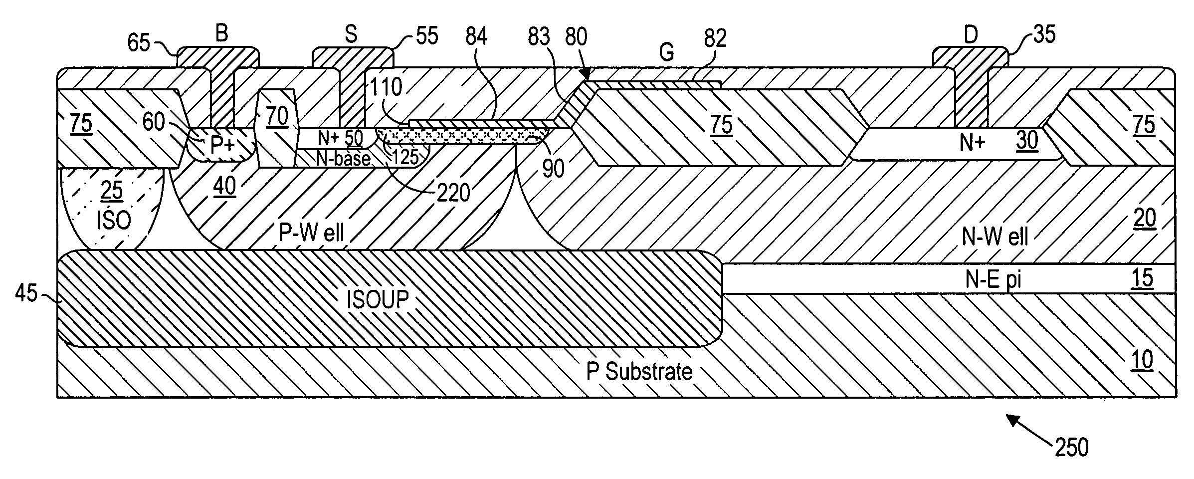
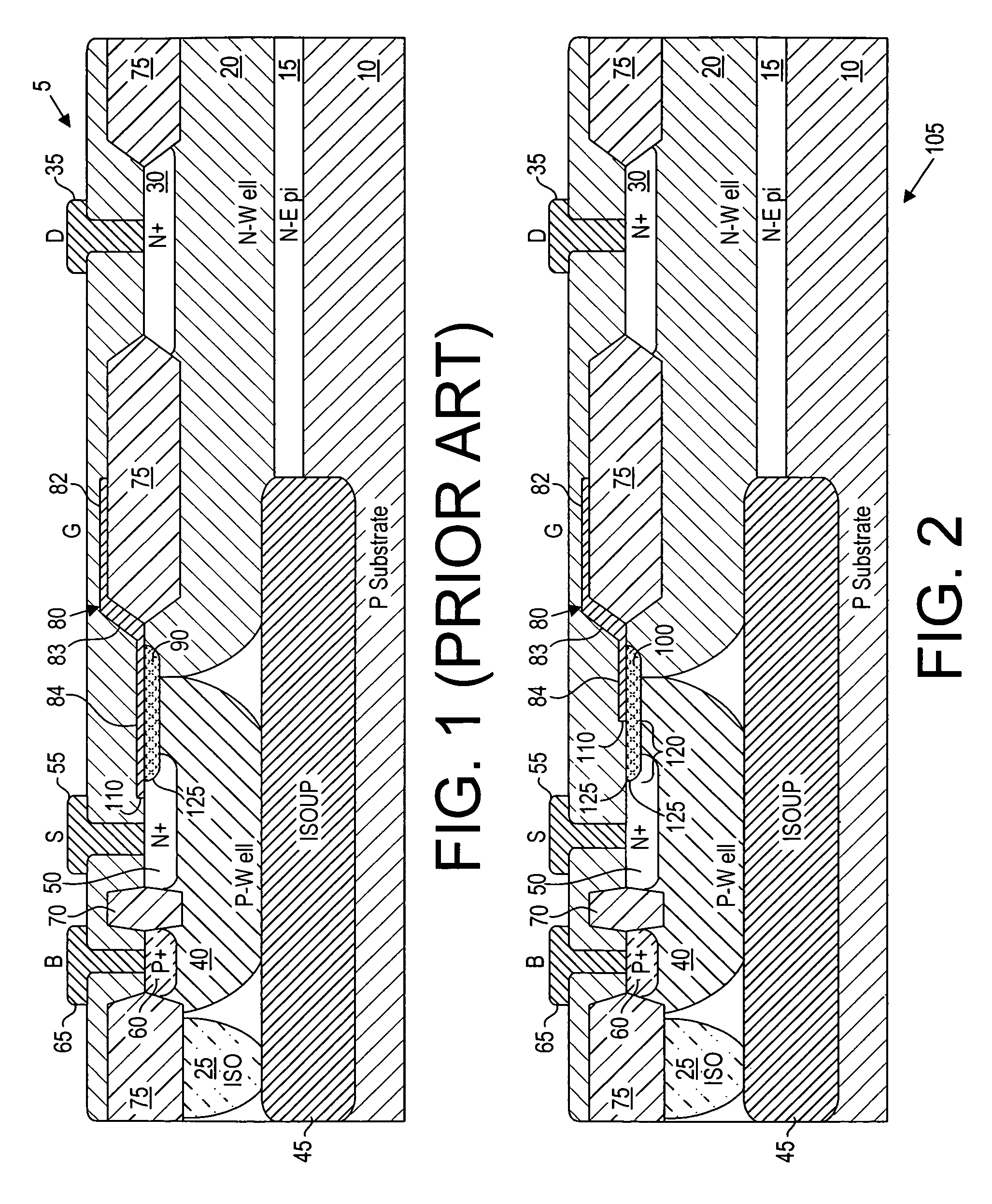
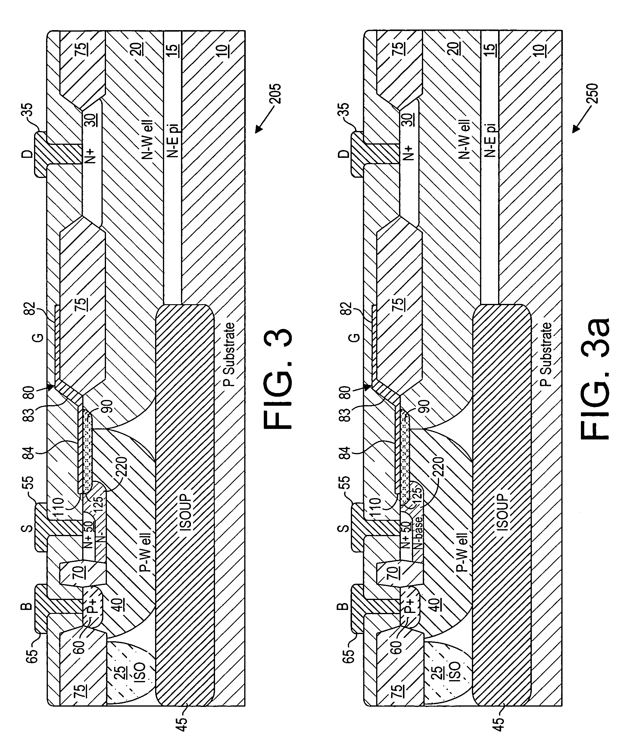
[0027]Referring to FIG. 2, an exemplary embodiment of a transistor within the present invention is illustrated. In particular, an LDMOS transistor 105 is shown, which has improved performance relative to LDMOS transistor 5 of FIG. 1. Common features of transistors 5 and 105 have the same reference numbers. While P-type semiconductor regions are referred to herein as first conductivity type regions, and N-type semiconductor regions are referred to herein as second conductivity type regions, the use of P-type and N-type semiconductor regions may be reversed. In the figures, heavily doped regions are depicted as N+ or P+, and more lightly doped regions are depicted with a N− or P−.

[0028]In one aspect, LDMOS transistor 105 achieves this improved performance compared to LDMOS transistor 5 of FIG. 1 through an extended depletion implant region 100 that functions as a source ballast resistor.

[0029]In particular, implant region 100 is of the second conductivity type, and is formed in a chan...


PUM


Abstract

A transistor is formed with a source ballast resistor that regulates channel current. In an LDMOS transistor embodiment, the source ballast resistance may be formed using a high sheet resistance diffusion self aligned to the polysilicon gate, and/or by extending a depletion implant from under the polysilicon gate toward the source region. The teachings herein may be used to form effective ballast resistors for source and/or drain regions, and may be used in many types of transistors, including lateral and vertical transistors operating in a depletion or an enhancement mode, and BJT devices.

Description

BACKGROUND OF THE INVENTION[0001]1. Technical Field[0002]The disclosure relates to integrated circuits, and in particular to transistors of integrated circuits.[0003]2. Discussion of the Related Art[0004]FIG. 1 shows a conventional depletion mode Lateral Double-diffused Metal-Oxide Semiconductor (LDMOS) transistor 5 that is fabricated on a silicon substrate 10. Substrate 10 is doped with a dopant of a first conductivity type, here a P-type dopant. An epitaxial layer 15 doped with a dopant of a second conductivity type, here an N-type dopant, is grown over substrate 10. A well 20 of the second conductivity type and a body region 40 of the first conductivity type are formed in epitaxial layer 15.[0005]A drain region 30, also of the second conductivity type, is formed in well 20 and is in contact with a drain electrode 35. Drain region 30 is doped with a higher concentration of the dopant of the second conductivity type that well 20.[0006]A source region 50 is formed within and abuts b...

Claims


Application Information

Patent Timeline
Patent Type & Authority Patents(United States)
IPC IPC(8): H01L23/58H01L29/94H01L27/07H01L29/08H01L29/78H02M7/00
CPCH01L27/0738H02M7/003H01L29/7816H01L29/0847H01L29/7838H01L29/086
Inventor MALLIKARJUNASWAMY, SHEKARALTER, MARTIN J.VINN, CHARLES L.
Owner MICREL
Why Eureka
Try Eureka