Dielectric loaded antenna apparatus with inclined radiation surface and array antenna apparatus including the dielectric loaded antenna apparatus

a technology of dielectric loading and antenna apparatus, which is applied in the direction of individual energised antenna arrays, resonant antennas, waveguide mouths, etc., can solve the disadvantage of antenna apparatus exhibiting an electric characteristic different from the desired electric characteristic, and is more difficult to adjust the installation position

Active Publication Date: 2006-08-08
PANASONIC INTELLECTUAL PROPERTY CORP OF AMERICA
View PDF11 Cites 31 Cited by
  • Summary
  • Abstract
  • Description
  • Claims
  • Application Information

AI Technical Summary

Benefits of technology

[0011]An essential object of the present invention is to provide a dielectric loaded antenna apparatus which can solve the above-mention...

Problems solved by technology

In a high frequency band such as a millimeter wave band, in particular, the loaded dielectric 108 and the radiation waveguide 7 are formed smaller, which makes it more difficult to adjust the installation positions.
If the installation positions are deviated, this leads to deterioration in gain and a change in main beam d...

Method used


Image

  • Dielectric loaded antenna apparatus with inclined radiation surface and array antenna apparatus including the dielectric loaded antenna apparatus
  • Dielectric loaded antenna apparatus with inclined radiation surface and array antenna apparatus including the dielectric loaded antenna apparatus
  • Dielectric loaded antenna apparatus with inclined radiation surface and array antenna apparatus including the dielectric loaded antenna apparatus

Examples


first preferred embodiment

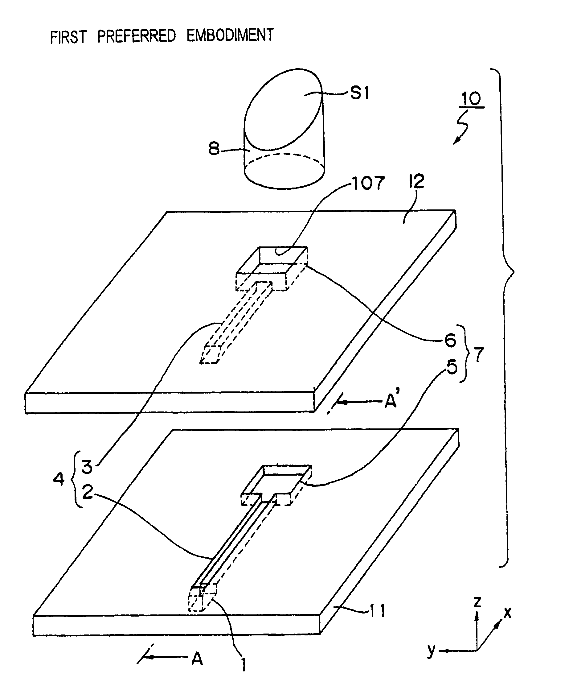
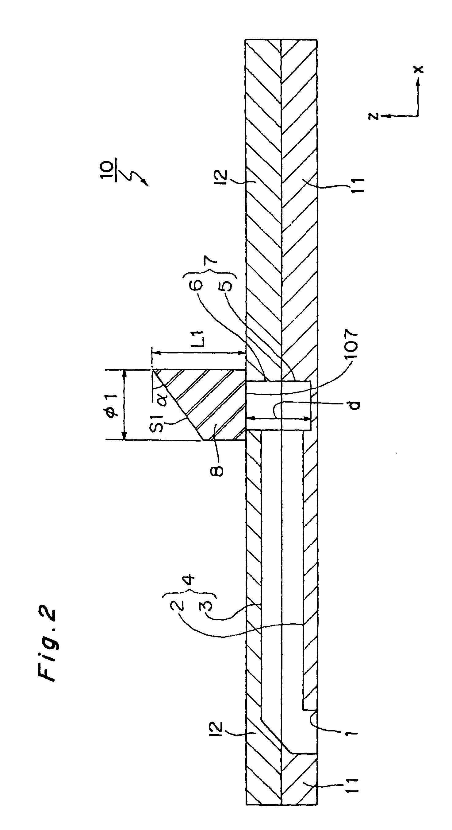
[0091]FIG. 1 is an exploded perspective view showing a configuration of a dielectric loaded antenna apparatus 10 of a first preferred embodiment according to the present invention. FIG. 2 is a longitudinal sectional view taken along a line A–A′ of FIG. 1. In all the preferred embodiments to be described later, an xyz coordinate system as shown in the drawings with a center of the radiation opening 107 of the radiation waveguide 7 set as an origin is referred to hereinafter, then the +z direction is referred to as an upper direction and the −z direction is referred to as a lower direction.

[0092]The loaded dielectric 108 of the conventional dielectric loaded antenna apparatus shown in FIG. 41 has a shape of circular column having a horizontal surface S0 as the top surface thereof, from which an electromagnetic wave is radiated and received. On the other hand, the dielectric loaded antenna apparatus 10 of the present preferred embodiment includes a circular-column-shaped loaded dielect...

second preferred embodiment

[0109]FIG. 8 is an exploded perspective view showing a configuration of a dielectric loaded antenna apparatus 10a of a second preferred embodiment according to the present invention. In the first preferred embodiment shown in FIGS. 1 and 2, the electromagnetic wave is fed by the feeding waveguide 4 and the radiation waveguide 7 provided on the lower conductor substrate 11 and the upper conductor substrate 12. The second preferred embodiment is characterized by feeding an electromagnetic wave by a microstrip line 17 formed on a dielectric substrate 14.

[0110]Referring to FIG. 8, a microstrip conductor 15 and a feeding patch conductor 16 are formed on the top surface of the dielectric substrate 14 having conductor layers formed on entire upper and bottom surfaces, respectively, by etching or the like using a pattern mask or the like. In this case, the feeding patch conductor 16 is electrically connected with the microstrip line 17 and the conductor layer formed on the bottom surface of...

third preferred embodiment

[0112]FIG. 9 is a longitudinal sectional view showing a configuration of a dielectric loaded antenna apparatus 10b of the third preferred embodiment according to the present invention while the arrangement of the loaded dielectric 8 and the radiation waveguide 7 is shown to be enlarged.

[0113]Referring to FIG. 9, the inclined surface S1 which is the top surface or the radiation surface of the loaded dielectric 8 is rotated on the xz plane and inclined at an inclination angle α2 from the plane parallel to the xy plane in a manner similar to that of the first preferred embodiment. Further, as compared with the arrangement of the first preferred embodiment, the central axis A2 of the loaded dielectric 8 parallel to the axial direction or the guide direction (the vertical direction) is arranged to be shifted by a displacement distance p in the +x direction from the central axis A1 of the radiation waveguide 7 parallel to the guide axial direction or the vertical direction. The central ax...


PUM


Abstract

A dielectric loaded antenna apparatus has a column-shaped loaded dielectric which is loaded on an end portion of a feeding line of the dielectric loaded antenna apparatus. The loaded dielectric has an inclined radiation surface which is inclined from a surface perpendicular to an axial direction of the loaded dielectric. A cross section of the loaded dielectric perpendicular to the axial direction of the loaded dielectric has a shape of one of a circle, ellipse and polygon. The feeding line is a waveguide which includes a radiation waveguide and a feeding waveguide. The radiation waveguide has an axis parallel to the axial direction of the loaded dielectric and includes an opening for feeding an electromagnetic wave to the loaded dielectric. The feeding waveguide feeds the electromagnetic wave to the radiation waveguide.

Description

BACKGROUND OF THE INVENTION[0001]1. Field of the Invention[0002]The present invention relates to a dielectric loaded antenna apparatus for use in a microwave band, a quasi-millimeter wave band, or a millimeter wave band, an array antenna apparatus including the dielectric loaded antenna apparatus, and a radio communication apparatus including one of the dielectric loaded antenna apparatus and the array antenna apparatus. In particular, the present invention relates to a dielectric loaded antenna apparatus with a loaded dielectric having an inclined radiation surface, an array antenna apparatus including the dielectric loaded antenna apparatus, and a radio communication apparatus including one of the dielectric loaded antenna apparatus and the array antenna apparatus.[0003]2. Description of the Related Art[0004]Conventionally, a dielectric loaded antenna apparatus having a loaded dielectric which is loaded on a feeder circuit which is constituted by a microstrip line, a waveguide or ...

Claims


Application Information

Patent Timeline
IPC IPC(8): H01Q1/38H01Q5/00H01Q9/04H01Q1/12H01Q3/24H01Q13/06H01Q13/10H01Q19/06H01Q21/06
CPCH01Q1/1221H01Q1/38H01Q3/24H01Q21/064H01Q13/06H01Q13/10H01Q19/06H01Q9/0485
Inventor OHNO, TAKESHIOGAWA, KOICHI
Owner PANASONIC INTELLECTUAL PROPERTY CORP OF AMERICA
Why Eureka
Try Eureka