System for detecting anomalies and/or features of a surface

a technology for anomalies and/or features, applied in the field of surface inspection systems, can solve problems such as false counts, inability to detect anomalies, and inability to accurately detect anomalies and/or features of surfaces, and achieve the effects of reducing the detection accuracy of surface anomalies

Inactive Publication Date: 2006-08-08
KLA TENCOR TECH CORP
View PDF26 Cites 55 Cited by
  • Summary
  • Abstract
  • Description
  • Claims
  • Application Information

AI Technical Summary

Benefits of technology

[0020]A surface inspection system with improved sensitivity and performance can be achieved by focusing a beam of radiation to illuminate a line on the surface of a sample and detecting scattered radiation from the line. When the surface inspection system is used to inspect samples with patterns such as arrays (e.g. memory arrays) thereon, the scattered radiation from the illuminated line is passed through a spatial filter prior to detection. In order to inspect the entire surface, relative motion is caused between the sample surface and the beam of radiation that illuminates the line on the surface. If the relative motion between the beam and the surface to inspect the whole surface is along straight lines, then the blocking pattern of the filter may be set after a learn cycle in order to shield the detector from the scattering from the pattern on the surface when there is such relative motion.
[0022]Instead of using a spatial filter in the above embodiments where relative motion between the sample surface and the illumination beam is along straight or curved lines, substantially the same effect can be achieved by reflecting the radiation scattered by the surface by means of strips of reflective material towards detectors, so that only scattered radiation that does not contain the diffracted components from the pattern on the surface is reflected to the detectors. Such and other variations are possible. Where the relative motion is along a curved line, the reflective strips may also be caused to shift (such as by switching) with the moving diffracted components.

Problems solved by technology

Such system requires significant time to scan the entire surface of a photomask or semiconductor wafer.
If the area illuminated is not the intended target area but is shifted relative to the target area, the comparison may yield false counts and may become totally meaningless.
Misregistration errors can be caused by misalignment of the illumination optics due to many causes such as mechanical vibrations, as well as by change in the position of the wafer such as wafer warp or wafer tilt or other irregularities on the wafer surface.
While the above-described systems may be satisfactory for some applications, they can be complicated and expensive for other applications.
In the inspection of samples with regular patterns thereon, the scattering from such patterns may overwhelm signals from anomalies of the sample.

Method used


Image

  • System for detecting anomalies and/or features of a surface
  • System for detecting anomalies and/or features of a surface
  • System for detecting anomalies and/or features of a surface

Examples


Embodiment Construction

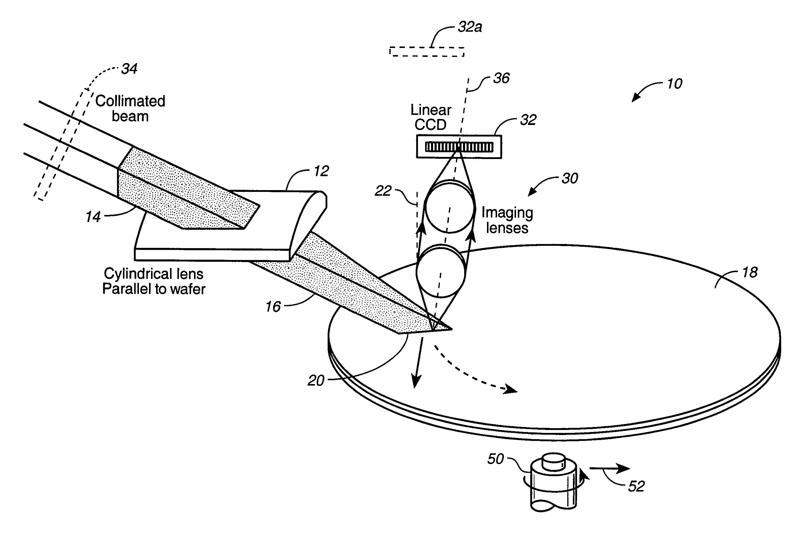
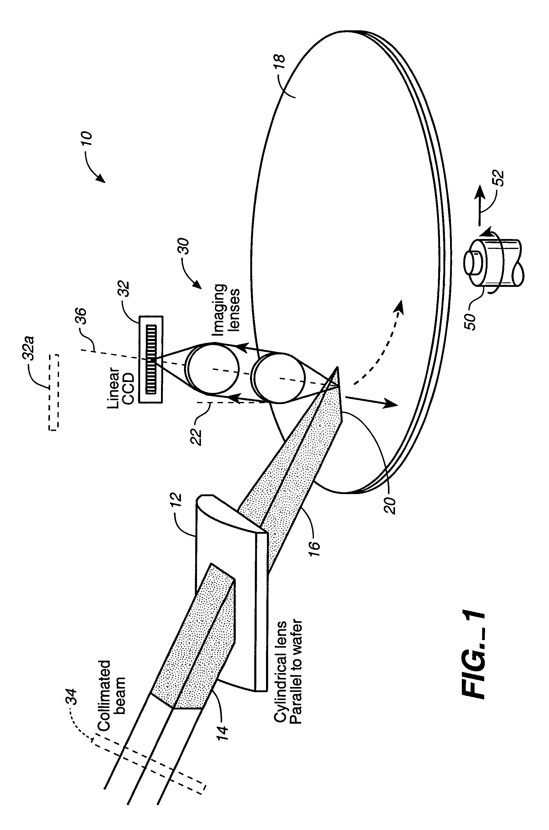
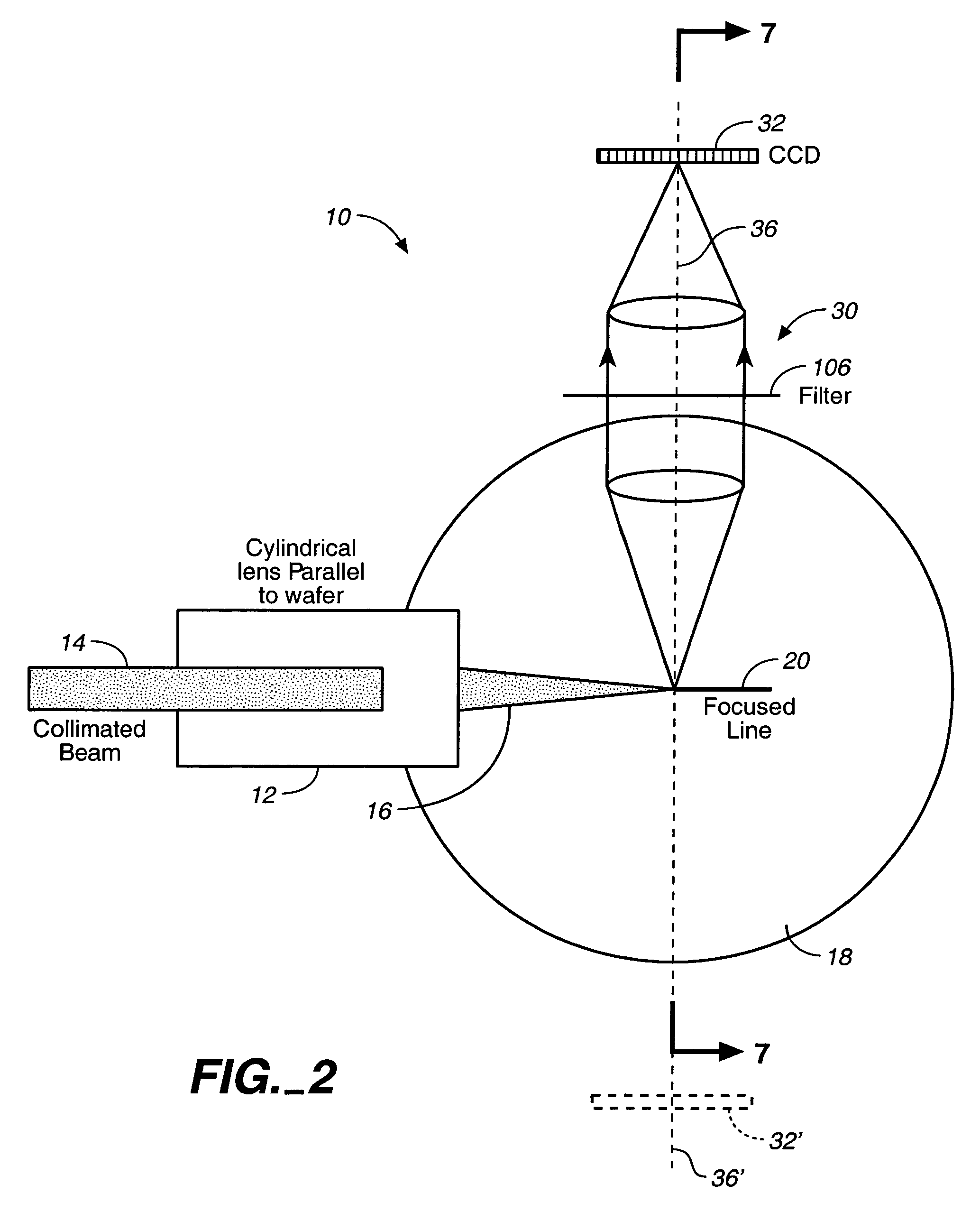
[0039]FIG. 1 is a perspective view of a surface inspection system to illustrate the preferred embodiment of the invention in the related application. System 10 includes a cylindrical objective such as a cylindrical lens 12 for focusing a preferably collimated light beam 14 to a focused beam 16 for illuminating, on surface 18 to be inspected, an area in the shape of a line 20. Beam 14 and therefore also focused beam 16 are directed at an oblique angle of incidence to the surface 18. Different from the approach by Gara described above, line 20 is substantially in the incidence plane or plane of incidence of focused beam 16. In this context, the incidence plane of beam 16 is defined by the common plane containing beam 16 and a normal direction such as 22 to surface 18 and passing through beam 16. In order for the illuminated line 20 to be in the focal plane of lens 12, cylindrical lens 12 is oriented so that its principal plane is substantially parallel to surface 18. Image of the line...


PUM

PropertyMeasurementUnit
oblique angleaaaaaaaaaa
lengthaaaaaaaaaa
widthaaaaaaaaaa

Abstract

A cylindrical mirror or lens is used to focus an input collimated beam of light onto a line on the surface to be inspected, where the line is substantially in the plane of incidence of the focused beam. An image of the beam is projected onto an array of charge-coupled devices parallel to the line for detecting anomalies and / or features of the surface, where the array is outside the plane of incidence of the focused beam. For inspecting surface with a pattern thereon, the light from the surface is first passed through a spatial filter before it is imaged onto the charge-coupled devices. The spatial filter includes stripes of scattering regions that shift in synchronism with relative motion between the beam and the surface to block Fourier components from the pattern. The spatial filter may be replaced by reflective strips that selectively reflects scattered radiation to the detector, where the reflective strips also shifts in synchronism with the relative motion.

Description

CROSS-REFERENCE TO RELATED APPLICATION[0001]This application claims the benefit of U.S. Provisional Application No. 60 / 356,500, filed Feb. 11, 2002, which application is incorporated by reference if fully set forth herein.BACKGROUND OF THE INVENTION[0002]This invention relates in general to surface inspection systems, and in particular, to an improved system for detecting anomalies and / or features of a surface.[0003]The need to detect anomalies of a surface such as those on the surface of a semiconductor wafer has been recognized since at least the early 1980's. In the article “Automatic Microcircuit and Wafer Inspection in Electronics Test,” May 1981, pp. 60–70, for example, Aaron D. Gara discloses a wafer inspection system for detecting whether microcircuit chips are placed upside down or not and for detecting flaws. In this system, a light beam from a laser is passed through a beam expander and a cylindrical lens having a rectangular aperture, where the lens focuses the beam to a...

Claims


Application Information

Patent Timeline
Patent Type & Authority Patents(United States)
IPC IPC(8): G01N21/00G01B11/30G01B11/24G01N21/47G01N21/94G01N21/95G01N21/956H01L21/66
CPCG01N21/47G01N21/95623G01N2201/1045G01N21/94
Inventor VAEZ-IRAVANI, MEHDIZHAO, GUOHENGSTOKOWSKI, STANLEY E.
Owner KLA TENCOR TECH CORP
Why Eureka
Try Eureka