
Optoelectronic device, and image sensor and electronic device including the same

an optoelectronic device and image sensor technology, applied in the manufacture of basic electric elements, radio frequency controlled devices, final product manufacturing, etc., can solve the problems of deteriorating the sensitivity the accuracy of the external quantum efficiency, and the low external quantum efficiency of the organic optoelectronic device in the visible light region, so as to improve the sensitivity and performance, the effect of reducing the dark curren

Active Publication Date: 2016-08-11
SAMSUNG ELECTRONICS CO LTD
View PDF4 Cites 3 Cited by
  • Summary
  • Abstract
  • Description
  • Claims
  • Application Information

AI Technical Summary

Benefits of technology

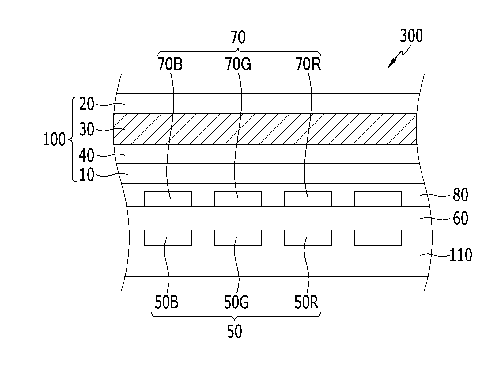
Example embodiments describe an optoelectronic device that reduces dark current and improves sensitivity and performance. This results in better image quality and a better overall experience for the user. The patent is also about an image sensor that utilizes this improved optoelectronic device.

Problems solved by technology

An organic optoelectronic device including a photoelectric conversion layer containing an organic material has relatively low external quantum efficiency in a visible light region and a relatively high dark current due to internal impurities in the organic material compared with an inorganic optoelectronic device including an inorganic oxide.
The relatively high dark current may increase the leakage current of the organic optoelectronic device, and thus deteriorate the sensitivity of the organic optoelectronic device as well as accuracy of the external quantum efficiency converted from a photocurrent during the photoreaction.

Method used


Image

  • Optoelectronic device, and image sensor and electronic device including the same
  • Optoelectronic device, and image sensor and electronic device including the same
  • Optoelectronic device, and image sensor and electronic device including the same

Examples


example 1

[0108]A 150 nm-thick first electrode is formed on a glass substrate by sputtering ITO. Subsequently, a 10 nm-thick first buffer layer including MoOx (x=2.62) is formed by thermally depositing molybdenum oxide on the first electrode and plasma-treating it under an oxygen atmosphere for 5 minutes. The x is verified through an AES (Auger electron spectroscopy) analysis. Herein, power is 100 W, and a gas flow rate is set to be 100 sccm. On the first buffer layer, an 80 nm-thick photoelectric conversion layer is formed by codepositing SubPC (a p-type semiconductor) and C60 (an n-type semiconductor) in a volume ratio of 1:1. Subsequently, on the photoelectric conversion layer, a 7 nm-thick second electrode is formed by thermally depositing ITO, manufacturing an optoelectronic device.

example 2

[0109]A 150 nm-thick first electrode is formed on a glass substrate by sputtering ITO. Subsequently, a 10 nm-thick first buffer layer including MoOx (x=2.78) is formed by thermally depositing molybdenum oxide on the first electrode and plasma-treating it under an oxygen atmosphere for 60 minutes. The x is verified through an AES (Auger electron spectroscopy) analysis. Herein, power is 100 W, and a gas flow rate is set to be 100 sccm. On the first buffer layer, an 80 nm-thick photoelectric conversion layer is formed by codepositing SubPC (a p-type semiconductor) and C60 (an n-type semiconductor) in a volume ratio of 1:1. Subsequently, a 7 nm-thick second electrode is formed by thermally depositing ITO on the photoelectric conversion layer, manufacturing an optoelectronic device.

[0110]Current densities of the optoelectronic devices according to Comparative Examples 1 and 2 and Examples 1 and 2 depending on a voltage are respectively measured, and the results are provided in FIG. 6. FI...


PUM


Abstract

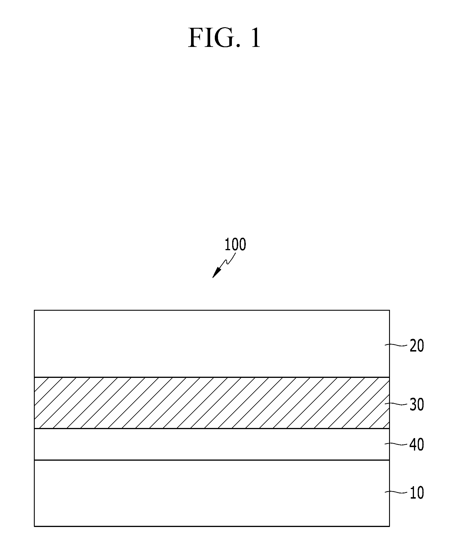
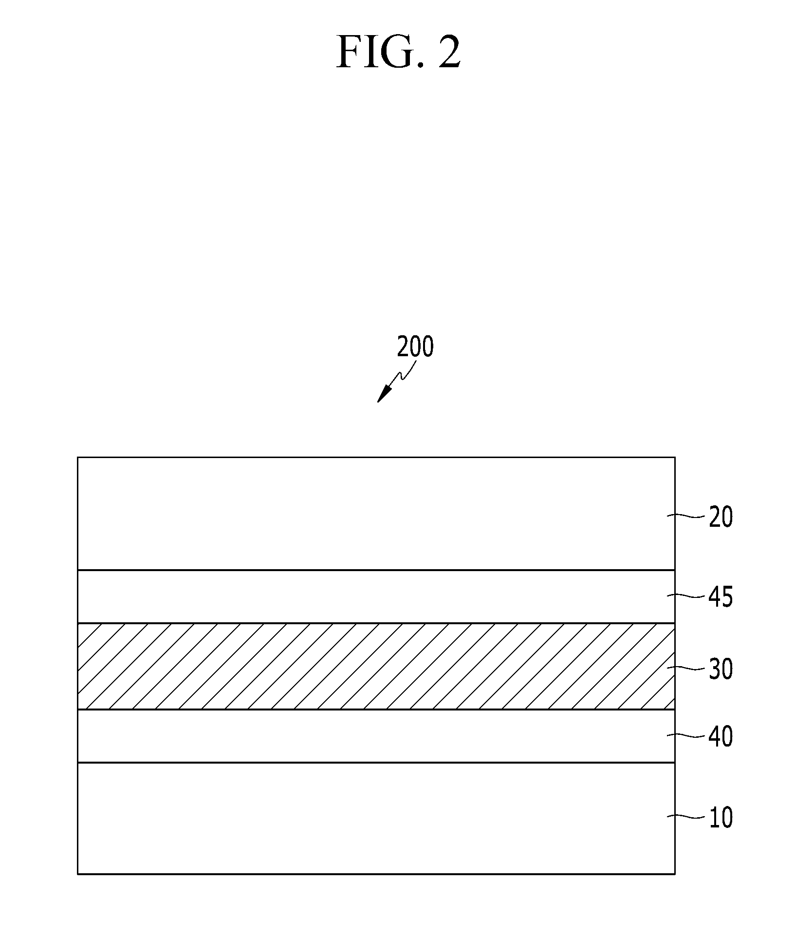
An optoelectronic device includes a first electrode and a second electrode facing each other, a photoelectric conversion layer between the first electrode and the second electrode, and a buffer layer between at least one of the photoelectric conversion layer and the first electrode, and the photoelectric conversion layer and the second electrode, the buffer layer including one of MoOx1 (2.58≦x1<3.0), ZnOx2 (1.0≦x2<2.0), TiOx3 (1.5≦x3<2.0), VOx4 (1.5≦x4<2.0), TaOx5 (1.0≦x5<2.5), WOx6 (2.0<x6<3.0), and a combination thereof.

Description

CROSS REFERENCE TO RELATED APPLICATION[0001]This application claims the benefit of priority from Korean Patent Application No. 10-2015-0018230 filed in the Korean Intellectual Property Office on Feb. 5, 2015, the entire contents of which are incorporated herein by reference.BACKGROUND[0002]1. Field[0003]Example embodiments relate to an optoelectronic device, and an image sensor and an electronic device including the same.[0004]2. Description of the Related Art[0005]An optoelectronic device is a device requiring a charge exchange between an electrode and a photoelectric conversion layer by using holes or electrons.[0006]An optoelectronic device may be classified as follows. A first optoelectronic device is an electronic device driven by generating excitons in a photoelectric conversion layer by photons from an external light source, separating the excitons into electrons and holes; and transferring the electrons and holes to different electrodes as a current source (voltage source). ...

Claims


Application Information

Patent Timeline
Patent Type & Authority Applications(United States)
IPC IPC(8): H01L31/0224H01L31/18H01L27/146
CPCH01L31/022408H01L31/18H01L27/14636Y02E10/549Y02P70/50H10K85/211H10K85/30H10K39/32H01L27/148H10K30/30
Inventor KIM, SEONG HEONYUN, DONGJINHEO, SUNGKIM, KYU SIKRYUICHI, SATOHPARK, GYEONGSULEE, HYUNG-IK
Owner SAMSUNG ELECTRONICS CO LTD
Learn More