Liquid crystal panel, apparatus for inspecting the same, and method of fabricating liquid crystal display thereof

a technology of liquid crystal panels and liquid crystal injection methods, which is applied in the direction of electrical testing, measurement devices, instruments, etc., can solve the problems of long time required for liquid crystal injection, difficult inspection of liquid crystal panels, so as to achieve less testing of individual liquid crystal panels

Inactive Publication Date: 2006-08-15
LG DISPLAY CO LTD
View PDF176 Cites 8 Cited by
  • Summary
  • Abstract
  • Description
  • Claims
  • Application Information

AI Technical Summary

Benefits of technology

[0039]An advantage of the present invention is to provide a composite liquid crystal panel having an electrode structure that enables electrical and visual inspection of the composite large liquid crystal panel. Another object of the present invention is to provide for an apparatus that inspects composite liquid crystal panels having a special electrode structure. Yet another object of the present invention is to provide a method of fabricating a composite liquid crystal display having a special electrode structure such that the composite liquid crystal display can be divided into individual liquid crystal panels, beneficial such that less testing of the individual liquid crystal panels is required.
[0040]Additional features and advantages of the invention will be set forth in part in the description which follows and in part will become apparent to those having ordinary skill in the art upon examination of the following or may be learned from practice of the invention. The objectives and other advantages of the invention may be realized and attained by the structure particularly pointed out in the written description and claims hereof as well as the appended drawings.
[0041]To achieve these and other advantages and in accordance with the purpose of the present invention, as embodied and broadly described herein, a liquid crystal panel according to the present invention includes a substrate having a plurality of substrate panels areas comprised of a plurality of perpendicularly crossing gate and data lines. Additionally, the substrate includes first and second metal lines that are respectively formed in the column and row directions and along edges of the substrate. A column-shorting bar that short-circuits a plurality of the gate lines is electrically connected to the second metal line. A row-shorting bar that short-circuits a plurality of the data lines is electrically connected to the first metal line.
[0042]In another aspect of the present invention, a method of fabricating a liquid crystal display includes preparing first and second substrates that, when bonded together, form a composite liquid crystal panel having a plurality of unit LC panel areas. The method further includes assembling the first and second substrates together by bonding, and then performing A / P testing that checks for electrical failures and visual defects of the composite liquid crystal panel.
[0043]In a further aspect of the present invention, fabricating a liquid crystal display includes the steps of preparing first and second substrates, each having a plurality of substrate panel areas, coating sealant around the substrate panel areas of one of the first and second substrates, dropping liquid crystals on the substrate panel areas of the other of the first and second substrates, forming a composite liquid crystal panel having a plurality of unit liquid crystal panel areas by bonding the first and second substrates together such that the substrate panel areas of the first and second substrates are opposed, carrying out A / P (auto probe) testing to identify electrical failures and visual defects in the unit large liquid crystal panel area, cutting the composite liquid crystal panel to form a plurality of individual liquid crystal panels, and then grinding faces of the individual liquid crystal panels.
[0044]In another further aspect of the present invention, an inspection apparatus includes a stage having a rotational axis that enables stage tilting, a light source inside the stage that enables substantially uniform light irradiation, a first polarizer arranged over the light source and dimensioned to cover a composite liquid crystal panel that is to be tested, and at least two voltage terminals for applying a predetermined voltage to the composite liquid crystal panel.

Problems solved by technology

While beneficial, liquid crystal injection using the foregoing procedures has problems.
For example, liquid crystal injection method requires a long time, such as over 10 hours to fill a ten-inch panel.
This problem is particularly acute when fabricating a large area LCD.
Additionally, the foregoing process wastes liquid crystal due to the fact that excess liquid crystal material cannot be reused because the liquid crystal may be contaminated and / or degraded by impurities and chemical reactions.
Notably, a liquid crystal injection inlet / opening is unnecessary.
Unfortunately, the liquid crystal dropping method has problems of its own.
That testing was relatively difficult and time consuming to perform since the drive lines of the all of the individual LC panels had to be driven with a predetermined pattern to test the individual LC panel.
This increases inspection time and leads to worker fatigue.

Method used


Image

  • Liquid crystal panel, apparatus for inspecting the same, and method of fabricating liquid crystal display thereof
  • Liquid crystal panel, apparatus for inspecting the same, and method of fabricating liquid crystal display thereof
  • Liquid crystal panel, apparatus for inspecting the same, and method of fabricating liquid crystal display thereof

Examples


Embodiment Construction

[0057]Reference will now be made in detail to illustrated embodiments of the present invention, examples of which are shown in the accompanying drawings. Wherever appropriate, the same reference numbers will be used throughout the drawings to refer to the same or similar parts.

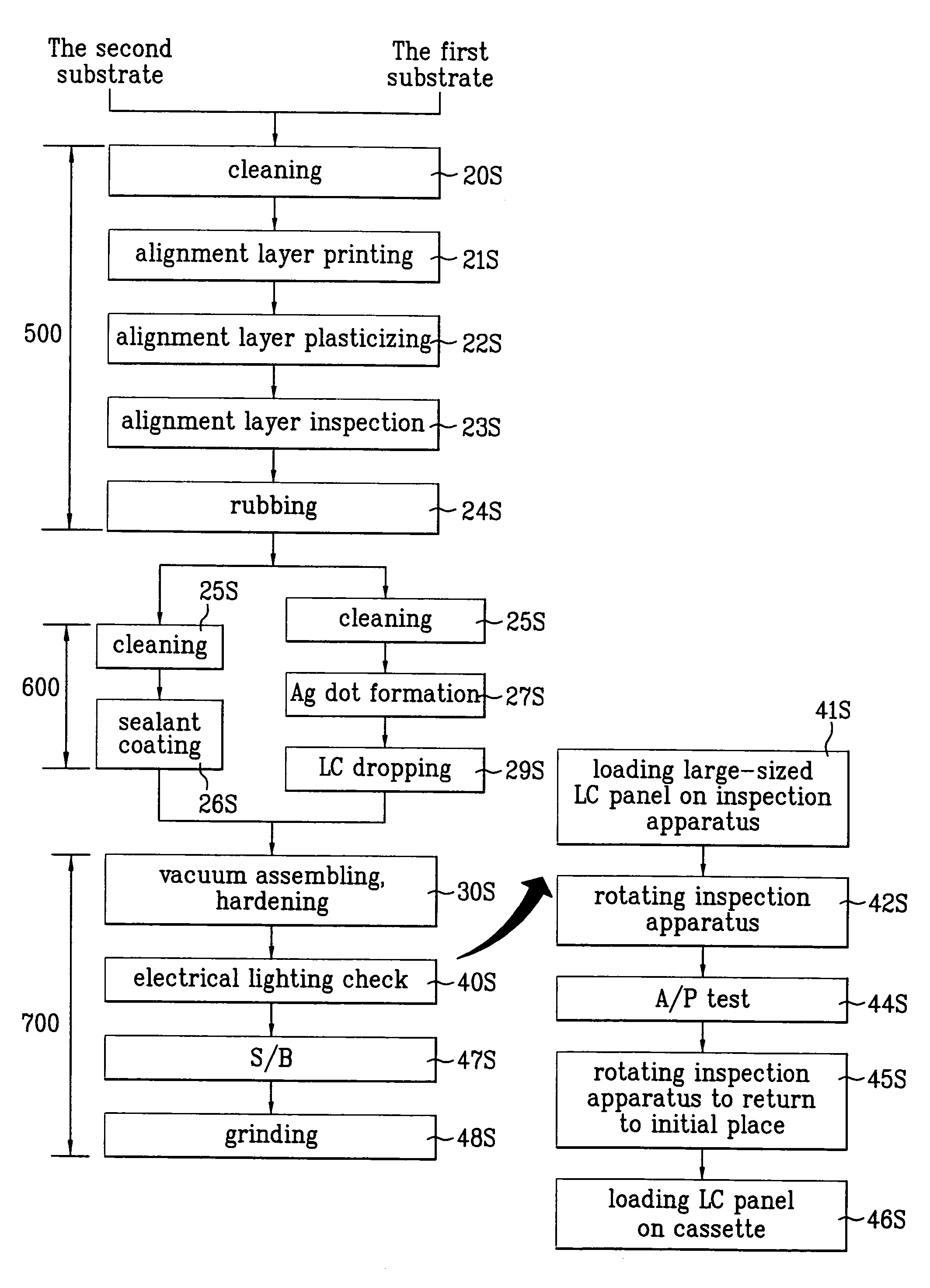
[0058]FIG. 4 schematically illustrates a first substrate of an LC panel according to an embodiment of the present invention, FIG. 5 schematically illustrates an unit LC panel area according to an embodiment of the present invention, FIG. 6 illustrates a magnified cross-sectional view of portion ‘A’ of FIG. 5, FIG. 7 illustrates a flowchart of an LCD fabrication method according to an embodiment of the present invention, FIG. 8 illustrates an inspection apparatus according to an embodiment of the present invention, and FIG. 9 schematically illustrates a structural layout of a composite LC panel according to an embodiment of the present invention.

[0059]Refer to FIG. 4 and FIG. 5 for illustrations of first and se...


PUM

PropertyMeasurementUnit
timeaaaaaaaaaa
areaaaaaaaaaaa
electrically testingaaaaaaaaaa

Abstract

A composite liquid crystal panel that interacts with an inspection station to simulate operating liquid displays, and methods of fabricating and testing such liquid crystal panels. The composite crystal panel enables the application of operating voltages to a plurality of unit liquid crystal panel areas. The inspection station provides operating power, illuminating light, and first and second polarizers. When power is applied to the composite liquid crystal panel an image is produced. That image will show defects in the unit liquid crystal panel areas. Beneficially, the inspection station tilts to enable easier problem identification.

Description

CROSS-REFERENCE TO RELATED APPIICATIONS[0001]This application is a divisional application of U.S. patent application No.: 10 / 184,103 filed Jun. 28, 2002, now U.S. Pat. No. 6,774,958; which claims priority to Korean Patent Application No.: 2002-0010197, filed Feb. 26, 2002 and Korean Patent Application No.: 2002-0013527, filed Mar. 13, 2002, each of which is incorporated by reference for all purposes as if fully set forth herein.[0002]This application incorporates by reference two co-pending applications, Ser. No. 10 / 184,096, filed on Jun. 28, 2002, entitled “SYSTEM AND METHOD FOR MANUFACTURING LIQUID CRYSTAL DISPLAY DEVICES” and Ser. No. 10 / 184,088, filed on Jun. 28, 2002, entitled “SYSTEM FOR FABRICATING LIQUID CRYSTAL DISPLAY AND METHOD OF FABRICATING LIQUID CRYSTAL DISPLAY USNG THE SAME”, as if fully set forth herein.BACKGROUND OF THE INVENTION[0003]1. Field of the Invention[0004]The present invention relates to liquid crystal display panels. In particular, the present invention ...

Claims


Application Information

Patent Timeline
Patent Type & Authority Patents(United States)
IPC IPC(8): G02F1/133G01R31/02G02F1/13G02F1/1333G02F1/1341G02F1/1345G02F1/1362
CPCG02F1/1309G02F1/133351G02F2001/136254G02F1/136254
Inventor KWEON, HYUG JINSON, HAE JOONKIM, WAN SOO
Owner LG DISPLAY CO LTD
Why Eureka
Try Eureka