Wavefront clock synchronization

Inactive Publication Date: 2006-08-15
NORMAN RICHARD S
View PDF7 Cites 10 Cited by
  • Summary
  • Abstract
  • Description
  • Claims
  • Application Information

AI Technical Summary

Benefits of technology

[0008]The present invention provides for the arrangement and management of timing various domains on a large integrated circuit which, to mitigate at least one of the problems of clock skew and the associated effects of slowing data propagation and reduction of clock frequencies, introduces a phase offset between clock domains of neighboring cells to create a wavefront clock which propagates through the circuit contemporaneously with data propagating though the circuit. The cells of the integrated circuit are synchronized to this wavefront clock in that the

Problems solved by technology

Electronic signals within large integrated circuits suffer from substantial propagation delays upon being transmitted across the circuit areas.
The propagation delays are a function of distance and are due to the parasitic reactances, the small but finite wire resistances and transistor switching times. The problem is further complicated by the fact that these delays are distributed across the area of the integrated circuit such that their effect on the propagation of the signals is typically not evenly felt everywhere within the area of the circuit.
This problem is commonly referred to as clock skew and leads to errors in the propagation of signals across the circuit.
Various approaches to skew compensation across a single large clock domain can be used, but these approaches typically suffer from inefficiencies in that once a sufficient clock skew has occurred data often must wait for subsequent clock cycles in order to propagate in phase with the clock.
Lowering the clock rate is, however, undesirable because it reduces the processing speed of the integrated circuit.
Half of the problem however rema

Method used


Image

  • Wavefront clock synchronization
  • Wavefront clock synchronization
  • Wavefront clock synchronization

Examples


Embodiment Construction

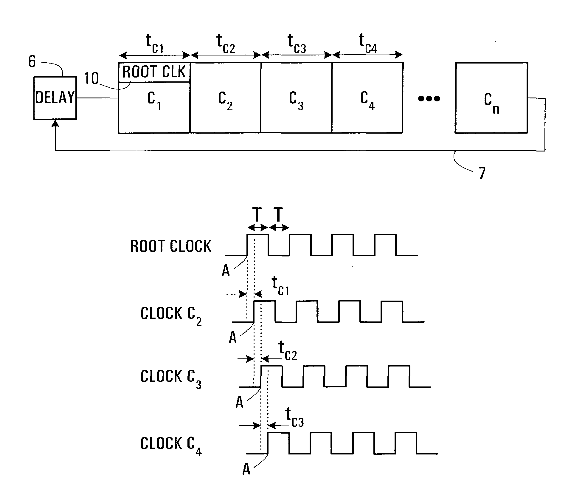
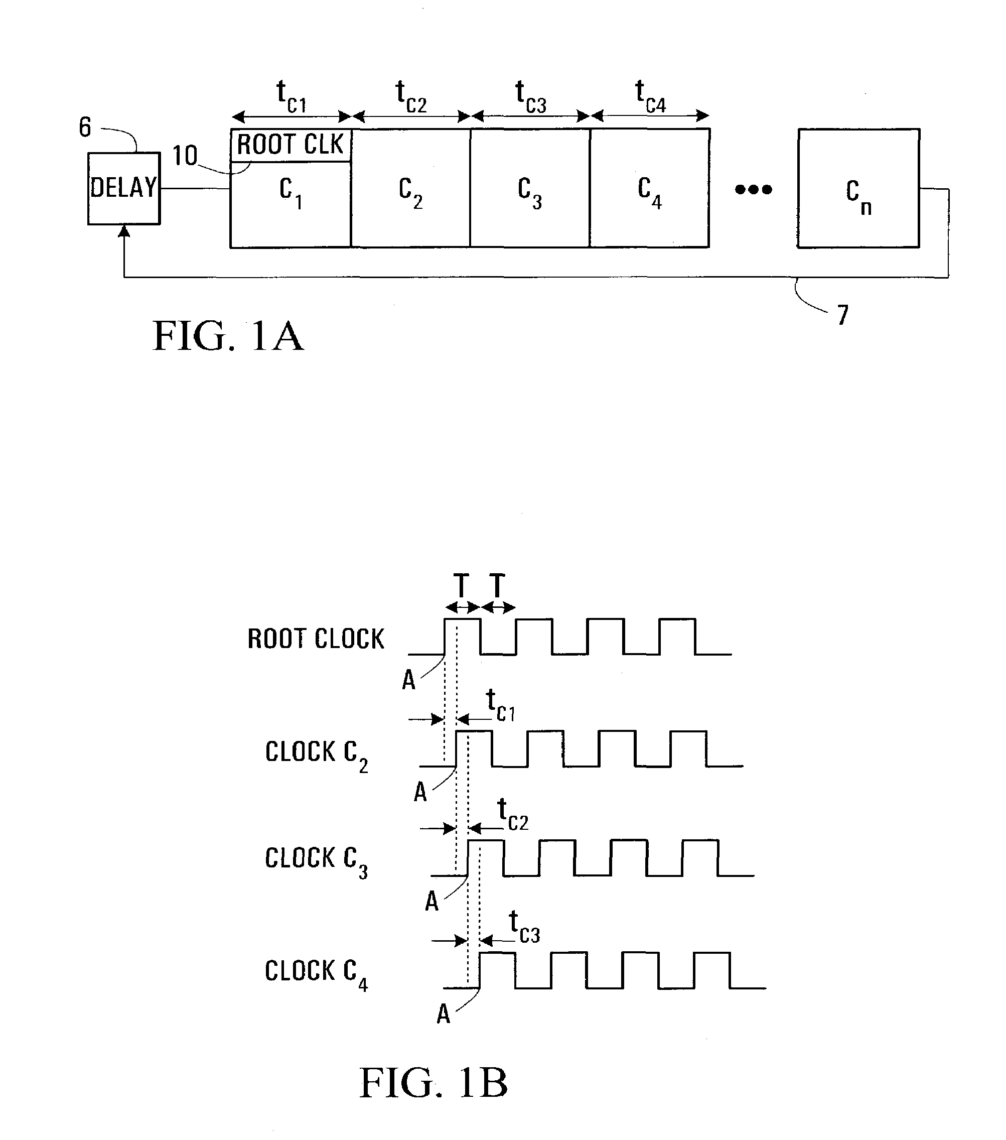
[0034]With reference to FIG. 1A, a row of integrated circuit cells timed according to one embodiment of the invention using one root clock 10, is described. The root clock 10 originates in cell C1 in which there is an associated propagation delay tc1. This means that the root clock signal upon reaching the rightmost boundary of cell C1 is out of phase (in time) with the source of the root clock signal by a delay or skew of tc1. Furthermore, since data moving across the cell also experiences substantially equivalent propagation delays to those experienced by the clock signal, the data signals will also be out of phase with their sources. Thus, synchronizing a clock in cell C2 or other cells to the root clock 10, at its source, causes the data and clock signals to move out of phase with each other. According to the embodiment depicted in FIG. 1A, the clock signal within cell C2 is deliberately set to be out of phase with the source of the root clock 10 by a time tC1 corresponding to t...


PUM


Abstract

The invention provides for the arrangement and management of timing of various domains on a large integrated circuit which introduces a phase offset between clock domains of neighboring cells to create a wavefront clock which propagates through the circuit at the same speed data propagates though the circuit. The cells of the integrated circuit are wavefront clock synchronized in that the phase offset introduced in a particular cell's clock is such that the arrival of a skewed clock and propagation delayed data from that cell's neighbor is synchronized with that particular cell's own clock. Wavefront clock synchronization mitigates at least some of the problems of clock skew and the associated effects of slowing data propagation and reduction of clock frequencies associated with large surface integrated circuits utilizing synchronized clock domains.

Description

CROSS-REFERENCES TO RELATED APPLICATIONS[0001]The present application claims the benefit under 35 USC 119(e) of prior U.S. Patent Application Ser. No. 60 / 343,165 to Richard Norman, filed on Dec. 31, 2001 and incorporated by reference herein.FIELD OF THE INVENTION[0002]The invention relates to timing on integrated circuits implemented on semiconductor wafers, and more particularly, to the arrangement and management of clock domains in cells of an integrated circuit.BACKGROUND OF THE INVENTION[0003]Electronic signals within large integrated circuits suffer from substantial propagation delays upon being transmitted across the circuit areas. The propagation delays are a function of distance and are due to the parasitic reactances, the small but finite wire resistances and transistor switching times. The problem is further complicated by the fact that these delays are distributed across the area of the integrated circuit such that their effect on the propagation of the signals is typical...

Claims


Application Information

Patent Timeline
IPC IPC(8): G06F1/12G06F1/04
CPCG06F1/10
Inventor NORMAN, RICHARDCHAMBERLAIN, DAVID
Owner NORMAN RICHARD S
Why Eureka
Try Eureka