
Method and apparatus using microscopic and interferometric based detection

a technology of interferometry and detection method, applied in the field of methods and systems, can solve the problems of difficult detection of defects sitting in dark structures, low signal level of dark structures, and inability to discriminate easily between slight perturbations and background, and achieve the effect of less sensitive to process nois

Active Publication Date: 2006-08-22
KLA TENCOR TECH CORP
View PDF9 Cites 31 Cited by
  • Summary
  • Abstract
  • Description
  • Claims
  • Application Information

AI Technical Summary

Benefits of technology

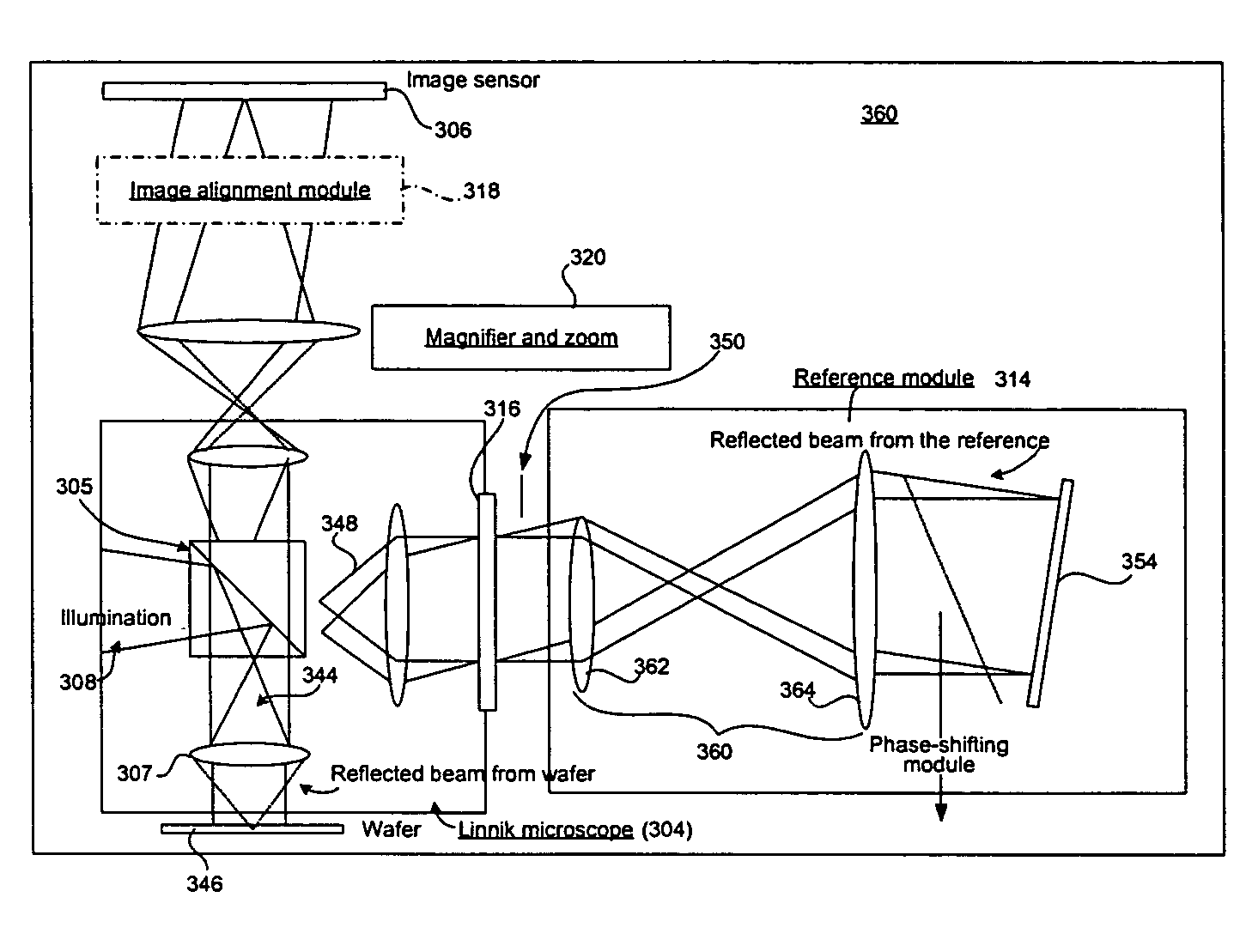
[0012]The present invention applies interferometric techniques to defect inspection, which is especially suitable for HARI, on semiconductor wafers in combination with intensity-based techniques. The interferometric techniques, as employed in embodiments of the present invention, can identify even subtle defects, such as those that generate very small intensity differences in comparison to the background. The phase-based techniques may be applied, for example, to wafers, masks, or reticles but are generally most suitable in detecting defects where the defects generate small intensity differences relative to a background. The integrated inspection tool also permits inspection using intensity based techniques for more distinct defects. Intensity based techniques are also less sensitive to process noise.

Problems solved by technology

With intensity based systems it is difficult to detect defects sitting in dark structures.
Because the background is darker, slight perturbations may not easily be discriminated against the background.
Furthermore, dark structures provide relatively low signal levels.
Moreover, other background noise, such as from misalignment between images for example, may mask slight differences in intensity attributable to the defect.
Laser scattering metrology techniques also rely on the interaction between the illumination and the defect structure, and therefore experience similar difficulties in identifying defects in high aspect ratio structures, i.e., high aspect ratio inspection (“HARI”).
As smaller geometries are used, the resulting smaller structures with smaller HARI will be difficult to detect with current tools.
Scanning electron microscopy (SEM) techniques are capable of inspecting HARI defects but are unsuitable for inspection inline.
SEM techniques are slow, and require that wafers must be taken off line for the inspection.
But phase measurement is not suitable for detecting all defects.
Phase based inspection techniques are especially suitable for small, subtle defects but aren't ideal in the presence of a signal having a strong intensity.
Phase measurements in such an application will create an abundance of problems.
A large defect may yield only a small phase defect signal.
Moreover, in identifying such defects, intensity based systems have lower throughputs and are more sensitive to pattern noise.

Method used


Image

  • Method and apparatus using microscopic and interferometric based detection
  • Method and apparatus using microscopic and interferometric based detection
  • Method and apparatus using microscopic and interferometric based detection

Examples


first embodiment

[0056]In the first embodiment, the tilt direction of the reference mirror (e.g., located within the reference module) is tilted to correspond to the direction of the stage scan. FIG. 11A is a diagram illustrating tilting of a reference mirror of an inspection system in accordance with one embodiment of the present invention. As illustrated, the reference mirror 1100 is shown titled along the x-axis. In order to maintain a constant OPD, the stage must cause the wafer scanning movement to occur also in the x direction. Stated another way, the tilting of the reference mirror along the x-axis may produce horizontal fringes 1105, as illustrated in the sample image on sensor 1110 depicted in FIG. 11B. FIG. 11B is a diagram illustrating a sample image appearing on a sensor in accordance with one embodiment of the present invention. Thus, alignment of the tilt direction of the reference mirror with the scanning direction x preserves the optical path difference. The stage movement causing th...

second embodiment

[0057]In a second embodiment employing the sensor TDI mode, optical path difference may be maintained by adjusting the location of the reference mirror in the z-direction to compensate for the optical path change in the reference beam path for each corresponding sensor pixel. FIG. 12A is a diagram illustrating tilting and movement of a reference mirror of an inspection system in accordance with another embodiment of the present invention. As illustrated, the reference mirror 1100 is tilted in the x direction, i.e., about the x-axis. This results in the formation of spatial fringes essentially parallel to a corresponding x axis of the sensor. That is, greater tilting of the mirror 1100 about its x axis increases the spacing between the parallel spatial fringe lines formed on the surface of the sensor while maintaining the direction of the fringe lines as parallel to the sensor's x axis. For purposes of this description, the surface of the sensor lies in the x-y plane of the sensor. I...


PUM


Abstract

An integrated interferometric and intensity based microscopic inspection system inspects semiconductor samples. A switchable illumination module provides illumination switchable between interferometric inspection and intensity based microscopic inspection modes. Complex field information is generated from interference image signals received at a sensor. Intensity based signals are used to perform the microscopic inspection. The system includes at least one illumination source for generating an illumination beam and an integrated interferometric microscope module for splitting the illumination beam into a test beam directed to the semiconductor sample and a reference beam directed to a tilted reference mirror. The beams are combined to generate an interference image at an image sensor. The tilted reference mirror is tilted with respect to the reference beam that is incident on the mirror to thereby generate fringes in the interference image. The system also includes an image sensor for acquiring the interference image from the inteferometric microscope module and intensity signals from the microscopic inspection image.

Description

CROSS-REFERENCE TO RELATED APPLICATIONS[0001]This application claims priority of U.S. Provisional Patent Application No. 60 / 414,750, filed 27 Sep. 2002, which application is incorporated herein by reference in its entirety for all purposes. This application is filed concurrently with and related to the following patent application: United States Nonprovisional application Ser. No. 10 / 672,298, entitled “METHOD AND APPARATUS USING INTERFEROMETRIC METROLOGY FOR HIGH ASPECT RATIO INSPECTION” naming Hwang et al. as inventors. The above-referenced United States patent application is incorporated herein by reference in its entirety for all purposes.BACKGROUND OF THE INVENTION[0002]The present invention relates generally to methods and systems for inspecting defects on wafers, masks, and reticles. More particularly, the present invention relates to optical inspection systems and techniques.[0003]In a conventional optical inspection system, defects are detected by subtracting a reference ima...

Claims


Application Information

Patent Timeline
IPC IPC(8): G01B11/02
CPCG01N21/95607G01B11/2441
Inventor HWANG, SHIOW-HWEICEGLIO, NAT
Owner KLA TENCOR TECH CORP
Learn More