Non-volatile semiconductor memory device

a non-volatile, memory device technology, applied in the direction of solid-state devices, transistors, instruments, etc., can solve the problems of non-volatile semiconductor memory devices that give rise to a large increase in the number of steps and costs, and the type of non-volatile semiconductor memory devices

Inactive Publication Date: 2006-08-22
KK TOSHIBA
View PDF15 Cites 14 Cited by
  • Summary
  • Abstract
  • Description
  • Claims
  • Application Information

AI Technical Summary

Problems solved by technology

Such a non-volatile semiconductor memory device, however, has inherent specifications, an element structure, and manufacturing processes and so has poor compatibility with the other logic products.
Therefore, this type of non-volatile semiconductor memory device gives rise to a great increase in number of steps and costs if it is to be integrated in the same semiconductor chip together with a peripheral logic circuit such as a CPU or an MPU.
The non-volatile semiconductor memory device, however, has the following problems.
The first problem is that it is not capable of electrical erasure.
That is, it is designed to erase the data by applying the ultraviolet light and so needs to use a package provided with a window fitted with quartz glass which transmits the ultraviolet light, which package, however, is very expensive.
The second problem is that the N type well needs to be independently provided for each memory cell, so that the cell becomes large in area.
Therefore, the memory device having such a large bit capacity cannot be formed in a semiconductor chip.

Method used


Image

  • Non-volatile semiconductor memory device
  • Non-volatile semiconductor memory device
  • Non-volatile semiconductor memory device

Examples


first embodiment

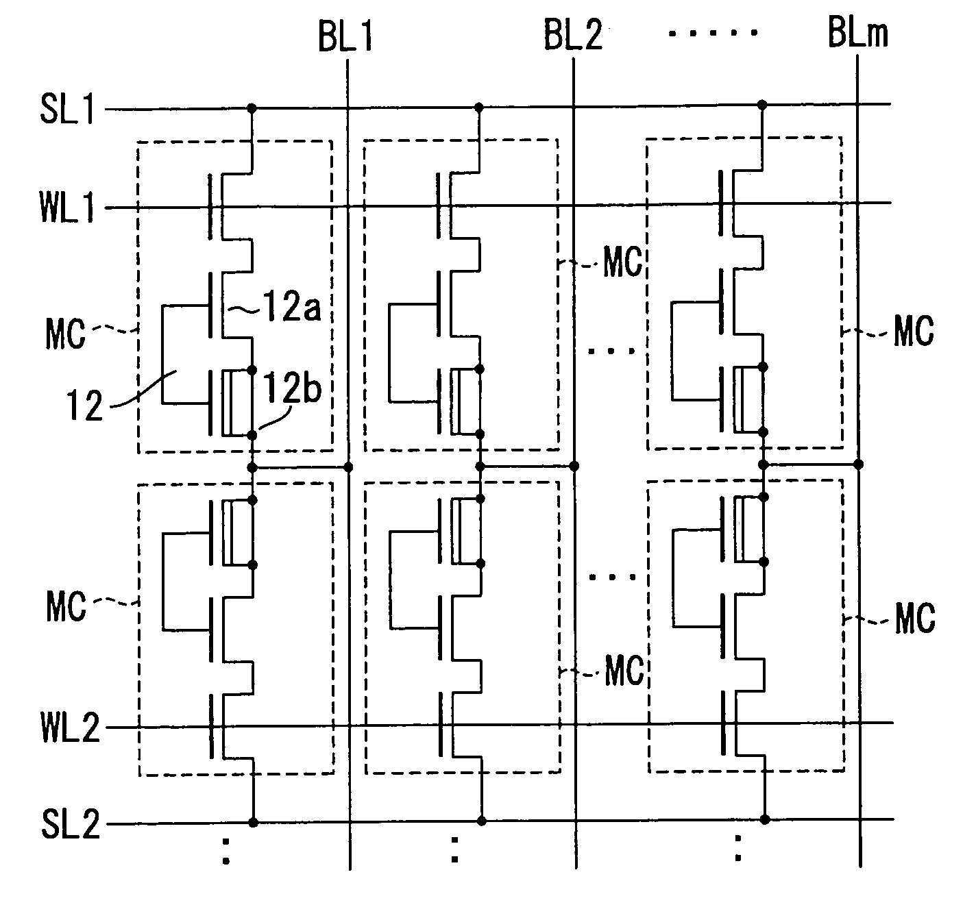
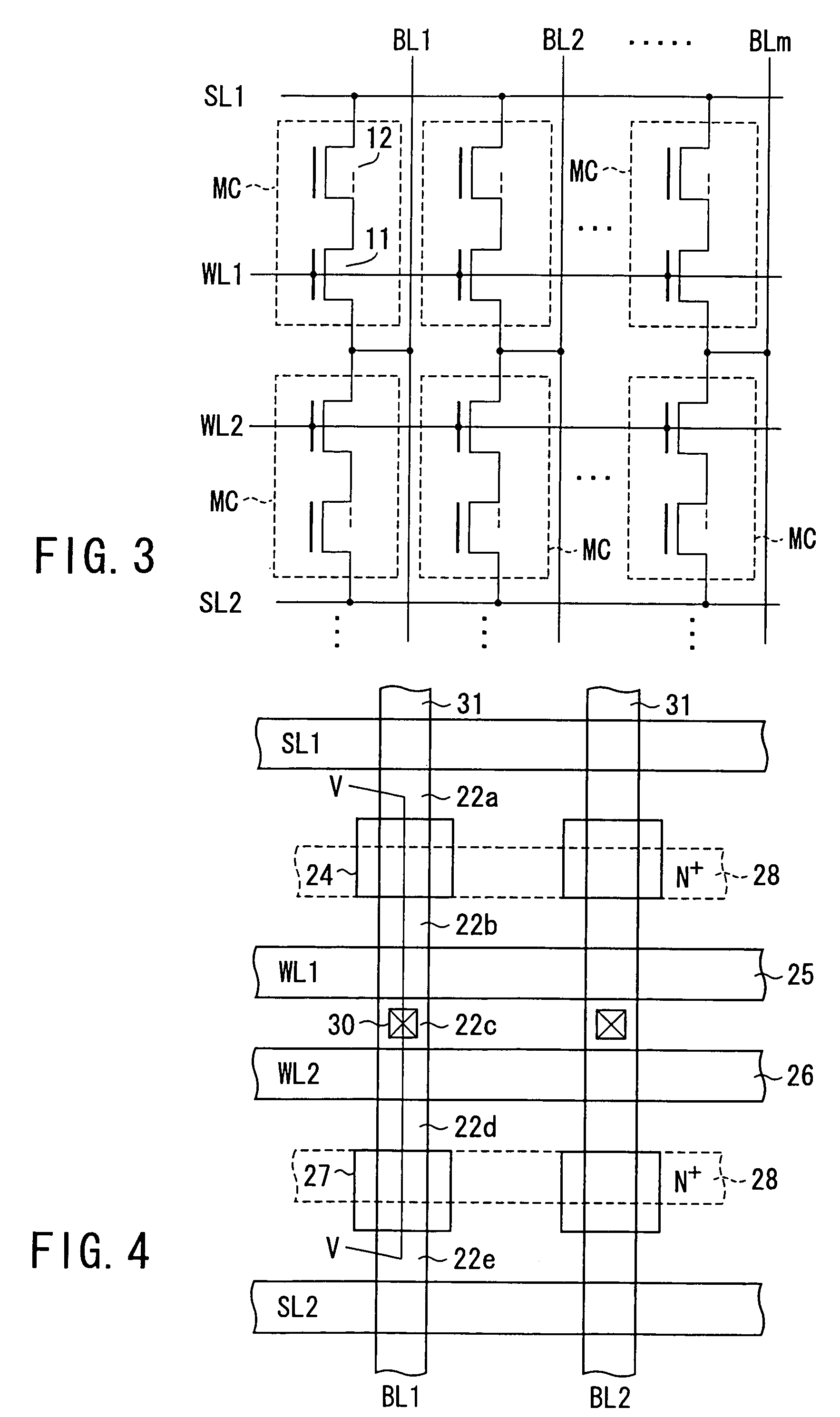
[0049]FIG. 3 is an equivalent circuit diagram which shows a configuration of part of a memory cell array of a non-volatile semiconductor memory device according to the first embodiment. As shown in it, a plurality of bit lines BL1, BL2 , . . . , BLm are arranged so as to extend in a first direction. Further, the respective pluralities of word lines and source lines are arranged so as to extend in a second direction which crosses the extension direction of the plurality of bit lines BL1, BL2 , . . . , BLm. It is to be noted that in FIG. 3, only the two word lines WL1 and WL2 and the two source lines SL1 and SL2 are shown.

[0050]At each intersection between each bit line BL and each source line SL, each memory cell MC is arranged. The memory cell MC has such a configuration that a selection transistor 11 constituted of an N-channel MOS transistor and a cell transistor 12 constituted of an N-channel MOS transistor are connected in series. A drain of the selection transistor 11 is connec...

second embodiment

[0084]FIG. 7 is an equivalent circuit diagram which shows a configuration of part of a memory cell array of a non-volatile semiconductor memory device according to a second embodiment. In the second embodiment also, as in the case of the first embodiment, the respective pluralities of bit lines, word lines, and source lines are arranged in such a configuration that a memory cell MC is placed at an intersection between each bit line BL and each source line SL. Further, each memory cell MC has such a configuration that a selection transistor 11 constituted of an N-channel MOS transistor and a cell transistor 12 constituted of an N-channel MOS transistor are connected in series.

[0085]A source region of the selection transistor 11 is connected to the corresponding source line SL (SL1 or SL2), while a gate electrode thereof is connected to the corresponding word line WL (WL1 or WL2). To a drain of the selection transistor 11 is there connected a source of the cell transistor 12. A drain ...

first modification

OF SECOND EMBODIMENT

[0115]The following will describe a first modification of the second embodiment.

[0116]FIG. 10 is a pattern plan view which shows some memory cells extracted from the memory cell array shown in FIG. 7. Components in FIG. 10 which corresponds to those in the pattern plan view of FIG. 8 are indicated by the same reference symbols and their explanation is omitted, to describe only the different components below.

[0117]The gates electrodes 24 and 27 of the cell transistor 12 have been described to each have the U-shaped plane geometry as shown in FIG. 8, in contract to which, however, in the case of the first modification, the gates 24 and 27 of the cell transistor 12 are rectangular in geometry. That is, in contrast to FIG. 8, the N+ diffusion regions 22C and 22E are omitted, so that the region where these N+ diffusion regions 22C and 22E have been present makes part of a channel region of the cell transistor 12. Further, an N+ diffusion region 28 is formed at one por...


PUM


Abstract

A memory cell has a selection transistor constituted of an MOS transistor having a gate electrode and a cell transistor constituted of an MOS transistor having the same polarity as the selection transistor, in such a configuration that these two transistors are connected in series. A bit line is connected to a drain region of the selection transistor and a word line is connected to the gate electrode thereof. A gate electrode of the cell transistor is not electrically connected anywhere so as to be in a floating potential state, while a drain region thereof is connected to a source region of the selection transistor. A source line is connected to a source region of the cell transistor.

Description

CROSS-REFERENCE TO RELATED APPLICATIONS[0001]The present application is a Divisional of U.S. application Ser. No. 10 / 434,080, filed on May 9, 2003, and in turn claims priority to Japanese Patent Applications No. 2002-135424, filed May 10, 2002; and No. 2003-100506, filed Apr. 3, 2003, the entire contents of each of which are incorporated herein by reference.BACKGROUND OF THE INVENTION[0002]1. Field of the Invention[0003]The present invention relates to a non-volatile semiconductor memory device which has non-volatile memory cells and which is especially suitable for being integrated in a semiconductor chip together with a peripheral logic circuit.[0004]2. Description of the Related Art[0005]Recently, on a user side constituting a semiconductor system, there increase demands for a non-volatile semiconductor memory device which is inexpensive and, capable of programming data after a semiconductor chip is manufactured. Such a non-volatile semiconductor memory device is required to be i...

Claims


Application Information

Patent Timeline
Patent Type & Authority Patents(United States)
IPC IPC(8): G11C16/04G11C5/06G11C16/02G11C16/06H01L21/8234H01L21/8247H01L27/06H01L27/088H01L27/10H01L27/105H01L27/115H01L29/788H01L29/792H01L31/109
CPCG11C16/0433H01L27/105H01L27/11558H01L27/11526H01L27/11529H01L27/11521H10B41/40H10B41/41H10B41/60H10B41/30G11C17/00
Inventor SHIROTA, RIICHIROSUGIMAE, KIKUKO
Owner KK TOSHIBA
Why Eureka
Try Eureka