Supercharge Your Innovation With Domain-Expert AI Agents!

Built-in self-test (BIST) of memory interconnect

a memory interconnect and self-testing technology, applied in the field of circuit testing, can solve the problems of memory chip defects, large bottleneck in properly testing such devices, and increase the complexity of integrated circuits (ics), and achieve the effect of efficient provision of instruction-based bist of external memory

Active Publication Date: 2006-08-22
ORACLE INT CORP
View PDF14 Cites 23 Cited by
  • Summary
  • Abstract
  • Description
  • Claims
  • Application Information

AI Technical Summary

Benefits of technology

[0014]The present invention includes novel methods and apparatus to efficiently provide instruction-based BIST of external memory. In an embodiment of the present invention, a method of testing a memory interconnect between an external memory module and a chip is disclosed. The method includes: providing an on-chip memory controller coupled to the external memory module, the on-chip memory controller sending and re

Problems solved by technology

As the complexity of integrated circuits (ICs) increases and access to their internal circuit nodes becomes harder, properly testing such devices becomes a major bottleneck during their prototyping, development, production, and maintenance.
Although the memory providers normally guarantee a reasonably high level of test coverage before shipping the memory chips to their customers, it is common to find defects in the memory chips after they are mounted on boards or modules.
Another category of failures can be attributed to interconnect defects.
Collective experience in the industry indicates that interconnect defects in general, and specifically memory interconnects, contribute significantly to failures on boards, modules and systems.
However, with the escalation of board operating frequencies and bus speeds at the connectors (sometimes reaching 150 MHz and beyond), the “stitching” introduces signal integrity or timing issues that render these techniques often unreliable or non-repeatable.
This fundamental problem results in higher test costs due to higher manufacturing retest rates, higher no-trouble found (NTF) rates, and / or higher test capital consumption.
This, in turn, requires a significant investment in expensive test hardware and test fixture capital.
Furthermore, while POST can be utilized as a board system level test feature, any enhancement to POST requires significant development time and cost.
This, along with the fact that POST development requires a “golden” board as a precondition, makes it logistically difficult to rely completely on POST enhancements to cover memory and memory interconnect test and diagnosis.
This increase in test costs has necessitated some fundamental changes in testing strategies for external memories and other board or system level components.
Not having to boot to a local OS relieves the requirement of having to “stitch” together a system with costly or unreliable invasive probing or interconnection techniques.
But having a memory test is not sufficient.
However, for example, today's DDR memories are usually not IEEE 1149.1 compliant and interconnects between such memories and other chips on a system or board are not tested well.
This approach offers a fair degree of flexibility but suffers from high area overhead.
However, this approach results in less flexibility of test algorithms and may not be applicable to many memory chips available on the market today.
Some of the issues with past EBIST techniques can be summarized as follows: (a) they require intrusion at a chip's IOs, which are usually in the critical paths, resulting in timing problems and design iterations to accommodate EBIST; (b) they require reimplementing the random access memory (RAM) access protocol inside the BIST engine, resulting in unnecessary area overhead (not to mention the risk of implementing and, hence, testing an incorrect protocol); and / or (c) they generally hardcode the test algorithm, the data background, and / or both, resulting in low test coverage of the memory subsystem and not providing the flexibility required for diagnosis or for targeting memories from different vendors.

Method used


Image

  • Built-in self-test (BIST) of memory interconnect
  • Built-in self-test (BIST) of memory interconnect
  • Built-in self-test (BIST) of memory interconnect

Examples


Embodiment Construction

[0023]In the following description, numerous details are set forth. It will be apparent, however, to one skilled in the art that embodiments of the invention may be practiced without these specific details. In other instances, well-known structures, devices, and techniques have not been shown in detail, in order to avoid obscuring the understanding of the description. The description is thus to be regarded as illustrative instead of limiting.

[0024]Reference in the specification to “one embodiment” or “an embodiment” means that a particular feature, structure, or characteristic described in connection with the embodiment is included in at least an embodiment of the invention. The appearances of the phrase “in one embodiment” in various places in the specification are not necessarily all referring to the same embodiment.

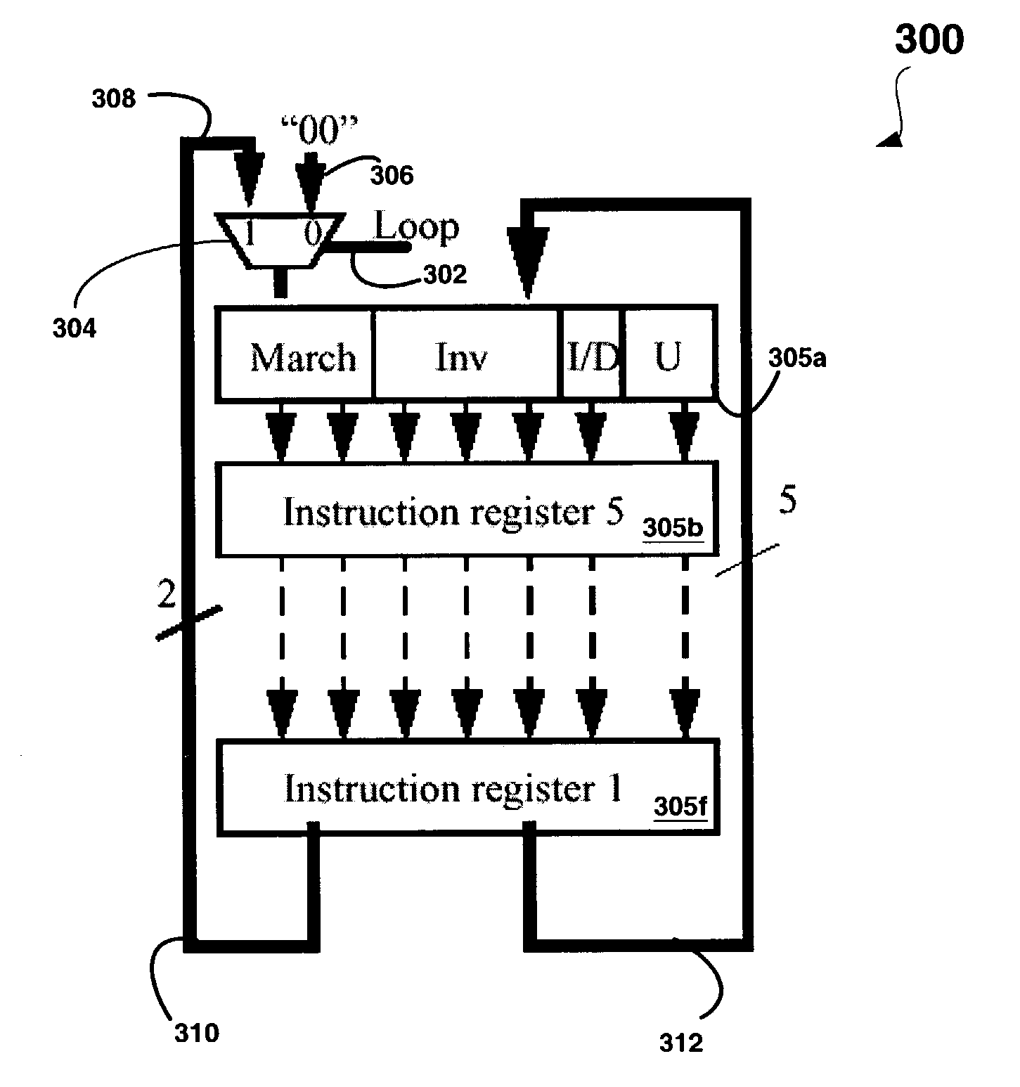
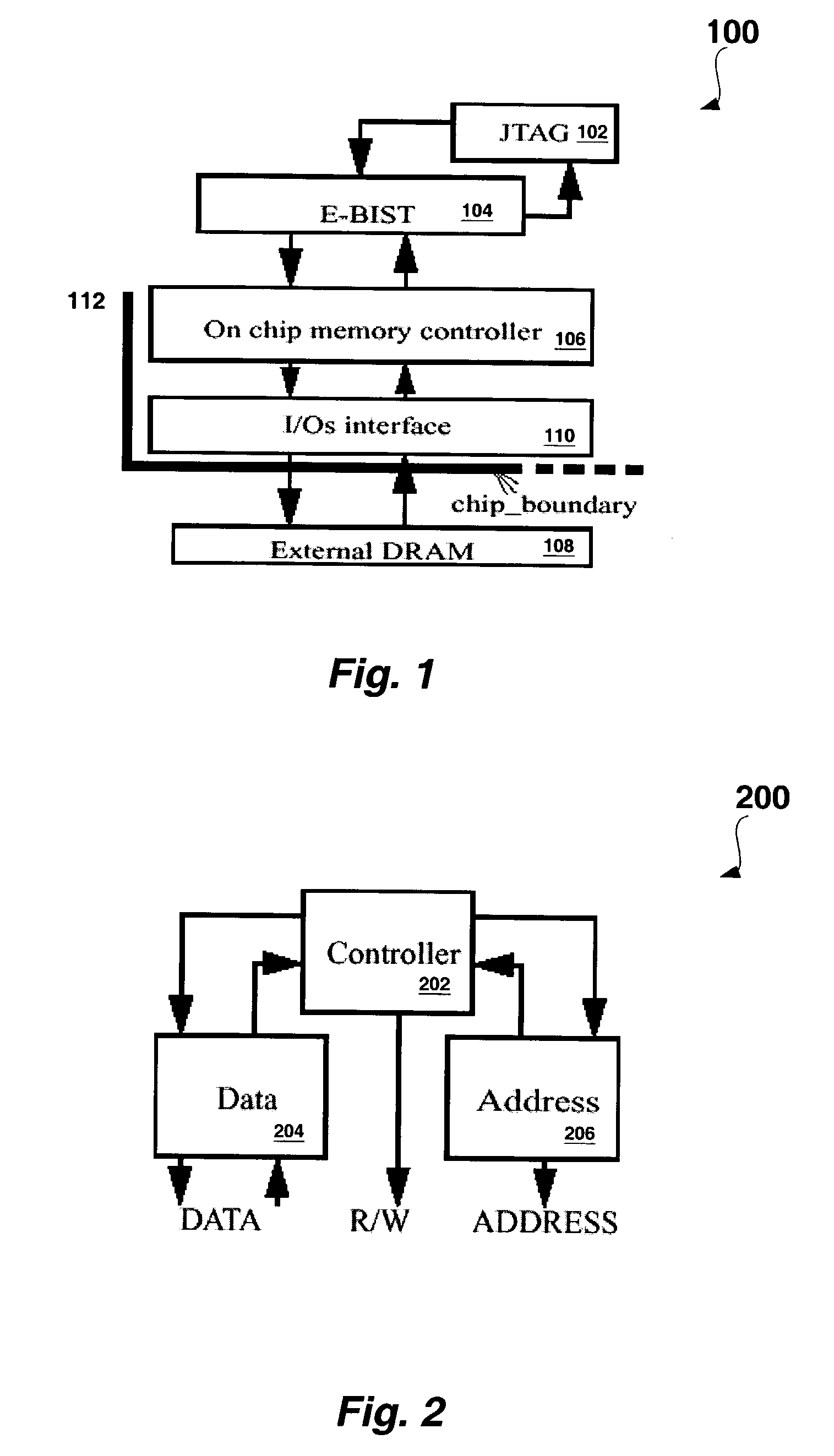
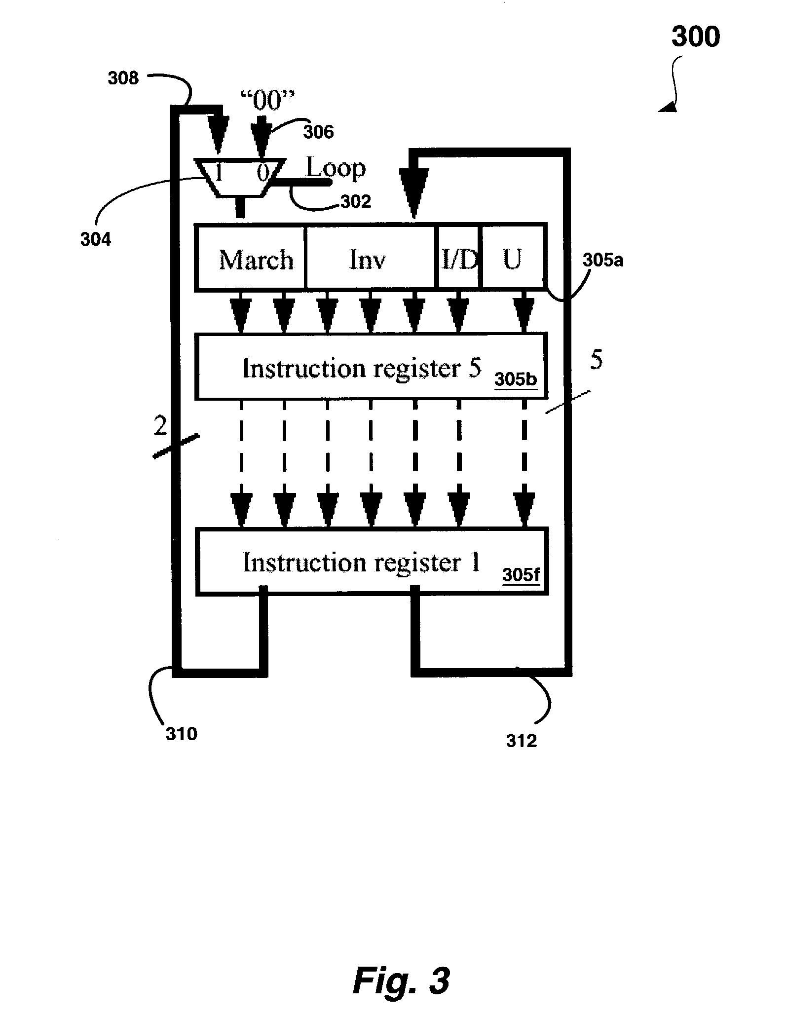
[0025]To provide access to BIST functionality on a chip, a test access port (TAP) may be utilized. TAP can be a general-purpose port that provides access to test suppo...


PUM


Abstract

Disclosed are novel methods and apparatus for efficiently providing instruction-based BIST of memory interconnects. In an embodiment of the present invention, a method of testing a memory interconnect between an external memory module and a chip is disclosed. The method includes: providing an on-chip memory controller coupled to the external memory module, the on-chip memory controller sending and receiving data to and from the external memory module; providing an on-chip built-in self-test (BIST) module coupled to the on-chip memory controller, the BIST module including an instruction register to store a plurality of instructions; testing the external memory module; and once the external memory module has successfully passed the testing, utilizing the external memory module in testing the memory interconnect.

Description

FIELD OF INVENTION[0001]The present invention generally relates to the field of circuit testing. More specifically, an embodiment of the present invention provides instruction-based built-in-self-test (BIST) of memory interconnects.BACKGROUND OF INVENTION[0002]As the complexity of integrated circuits (ICs) increases and access to their internal circuit nodes becomes harder, properly testing such devices becomes a major bottleneck during their prototyping, development, production, and maintenance. As a result, designs with BIST implementation have become commonplace. In a BIST implementation, circuitry (which is intended solely to support testing) is included in an IC or in a system including ICs.[0003]With 64-bit support in the latest generation of microprocessor families, it is customary to find large (e.g., up to 40 GB) external memories and associated interconnects. Although the memory providers normally guarantee a reasonably high level of test coverage before shipping the memor...

Claims


Application Information

Patent Timeline
IPC IPC(8): G11C29/00G01R31/28G11C29/16
CPCG11C29/022G11C29/16G11C2029/3602
Inventor CATY, OLIVIERBAYRAKTAROGLU, ISMETMAJUMDAR, AMITAVA
Owner ORACLE INT CORP
Features
  • R&D
  • Intellectual Property
  • Life Sciences
  • Materials
  • Tech Scout
  • Unparalleled Data Quality
  • Higher Quality Content
  • 60% Fewer Hallucinations
Learn More