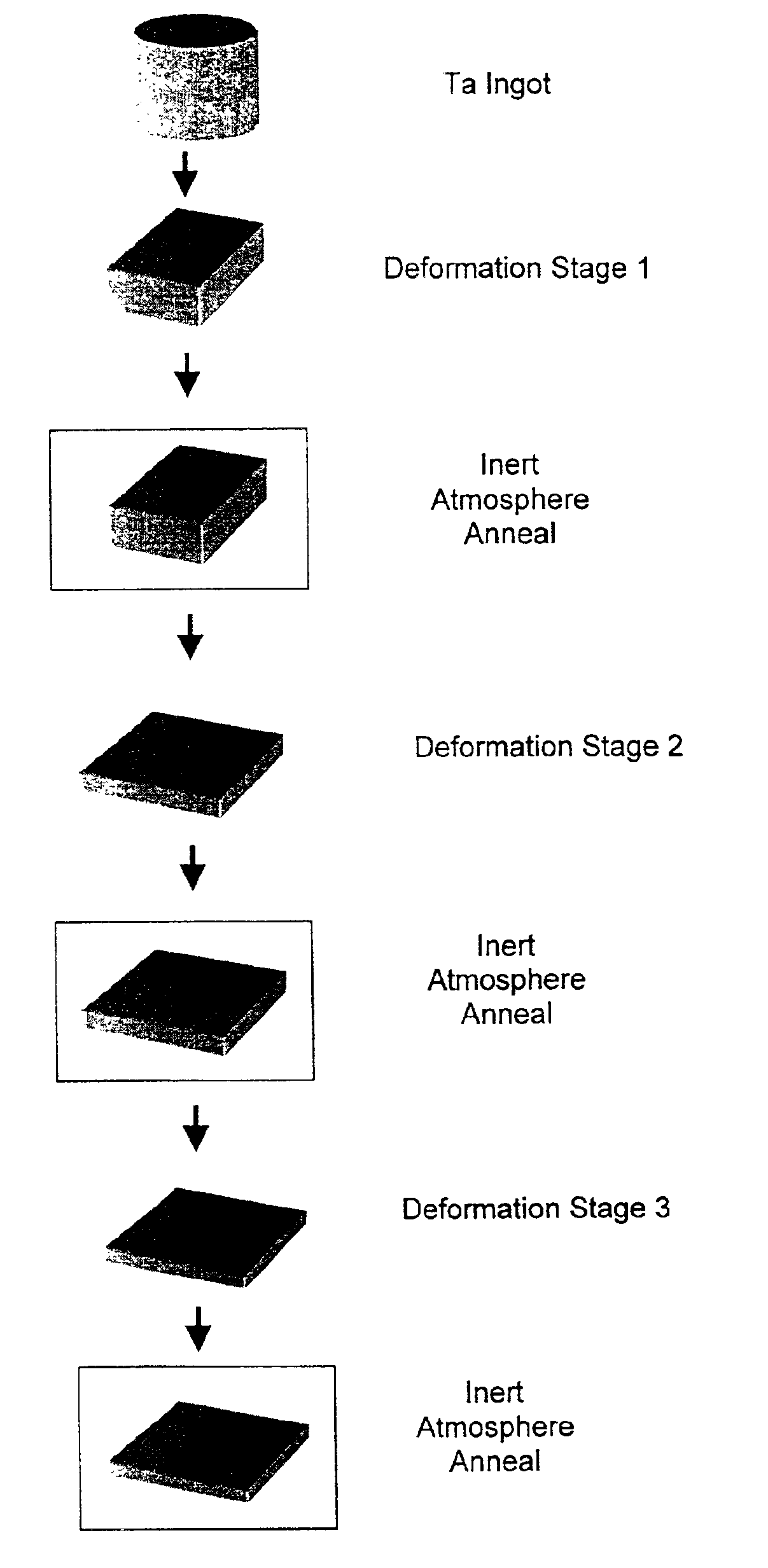
Tantalum sputtering target with fine grains and uniform texture and method of manufacture
- Summary
- Abstract
- Description
- Claims
- Application Information
AI Technical Summary
Benefits of technology
Problems solved by technology
Method used
Image

Examples
Example
EXAMPLE 1
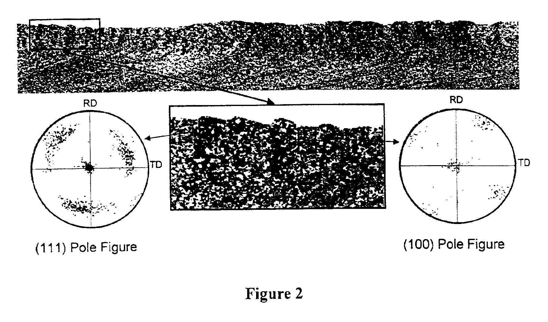
[0024]Twelve high-purity tantalum ingots were processed according to conventional methods or the process of this invention. The parameters for each experiment and the corresponding grain size and texture results are summarized in Table 1. Texture uniformity was measured by cutting samples from the target and analyzing them using an EBSD system on a scanning electron microscope (SEM). The mapped area was 7 mm×7 mm and was measured from the target surface to at least the plate mid-thickness. The lighter areas depict {111} textures and the darker areas depict {100} textures.
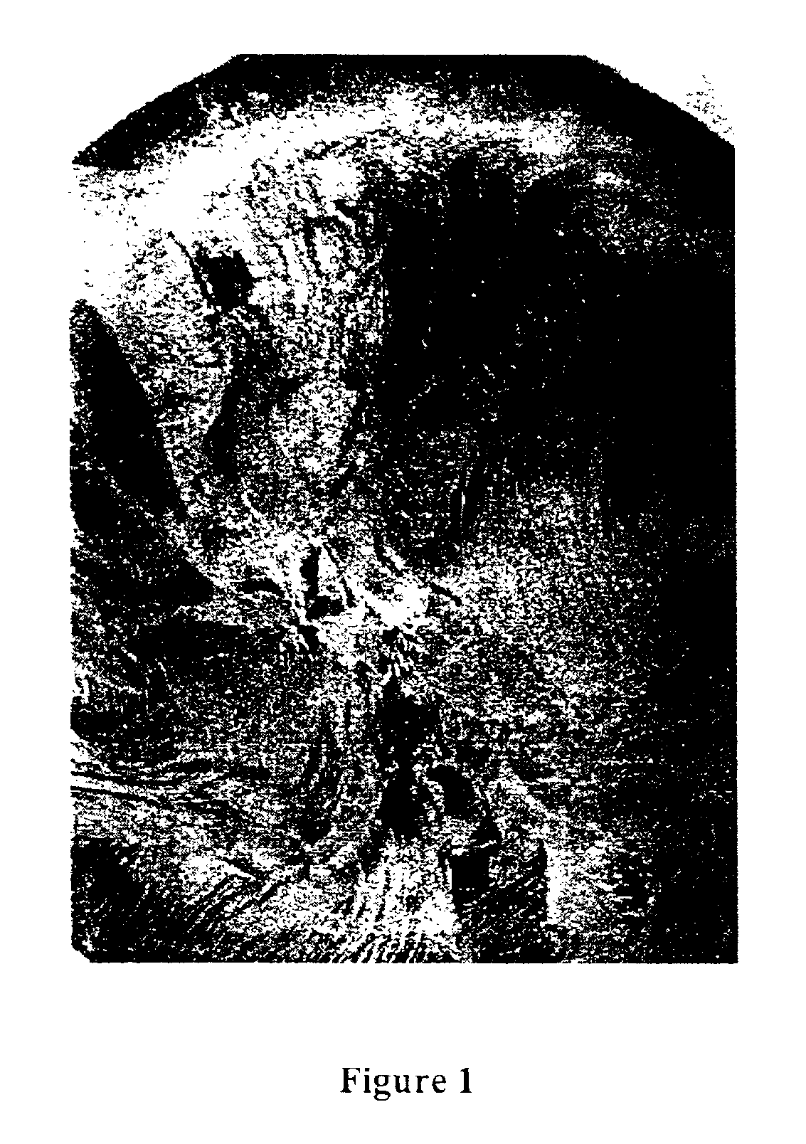
[0025]The ingots processed by conventional methods (Processes 1 through 7) exhibited a banded microstructure in both grain size and texture. FIGS. 4, 5, 6 and 7 illustrate the extent of this banding. The ingots manufactured by the invented process (Processes 8 through 12) have a strong {111} textures with a random distribution of {100} textures. FIG. 8, which represents product of the present invention, sho...
Example
EXAMPLE 2
[0028]Sputter trials were conducted on a conventional high-purity tantalum target and a target processed according to this invention in order to compare the sputtering characteristics. FIG. 9(a) and FIG. 9(b) are photographs of the used conventional and invented targets, respectively. The conventional target exhibits extensive surface roughness which is associated with non-uniform sputtering. This surface ‘ridging’ in turn increases the likelihood of micro-arcing and sputter film non-uniformity. In contrast, the target processed according to this invention exhibits a smooth evenly-sputtered surface.
PUM
| Property | Measurement | Unit |
|---|---|---|
| Grain size | aaaaa | aaaaa |
| Temperature | aaaaa | aaaaa |
| Temperature | aaaaa | aaaaa |
Abstract
Description
Claims
Application Information
 - R&D Engineer
- R&D Manager
- IP Professional
- Industry Leading Data Capabilities
- Powerful AI technology
- Patent DNA Extraction
Browse by: Latest US Patents, China's latest patents, Technical Efficacy Thesaurus, Application Domain, Technology Topic.
© 2024 PatSnap. All rights reserved.Legal|Privacy policy|Modern Slavery Act Transparency Statement|Sitemap