Laser apparatus, laser annealing method, and manufacturing method of a semiconductor device

a manufacturing method and laser annealing technology, applied in the direction of semiconductor devices, electrical equipment, basic electric elements, etc., can solve the problems of increasing production cost, increasing production cost, and many of the attachments are also expensive, and achieve the effect of reducing the q value of laser resonators, high energy value, and significantly less running cost of solid-state lasers

Inactive Publication Date: 2005-12-13
SEMICON ENERGY LAB CO LTD
View PDF41 Cites 132 Cited by
  • Summary
  • Abstract
  • Description
  • Claims
  • Application Information

AI Technical Summary

Benefits of technology

[0011]The present invention has been made in view of the above, and an object of the present invention is therefore to provide a laser apparatus which is capable of providing a crystalline semiconductor film with a larger crystal grain size than in prior art and which is low in running cost, and to provide a laser annealing method using that laser apparatus. Another aspect of the present invention is to provide a semiconductor device fabricated by using the laser annealing method and a method of manufacturing the semiconductor device.

Problems solved by technology

However, Kr (krypton) gas and Xe (xenon) gas are very expensive, causing a problem of increase in production cost when recharge of the gas is frequent.
Many of these attachments are also expensive, taking part in increasing the production cost.
As seen in the above, a laser apparatus using excimer laser light does possess high ability but also possess drawbacks in that maintenance thereof is very troublesome and that the running cost (which means the costs required for operating the apparatus) is high for a laser apparatus for mass production.

Method used


Image

  • Laser apparatus, laser annealing method, and manufacturing method of a semiconductor device
  • Laser apparatus, laser annealing method, and manufacturing method of a semiconductor device
  • Laser apparatus, laser annealing method, and manufacturing method of a semiconductor device

Examples


embodiment mode 1

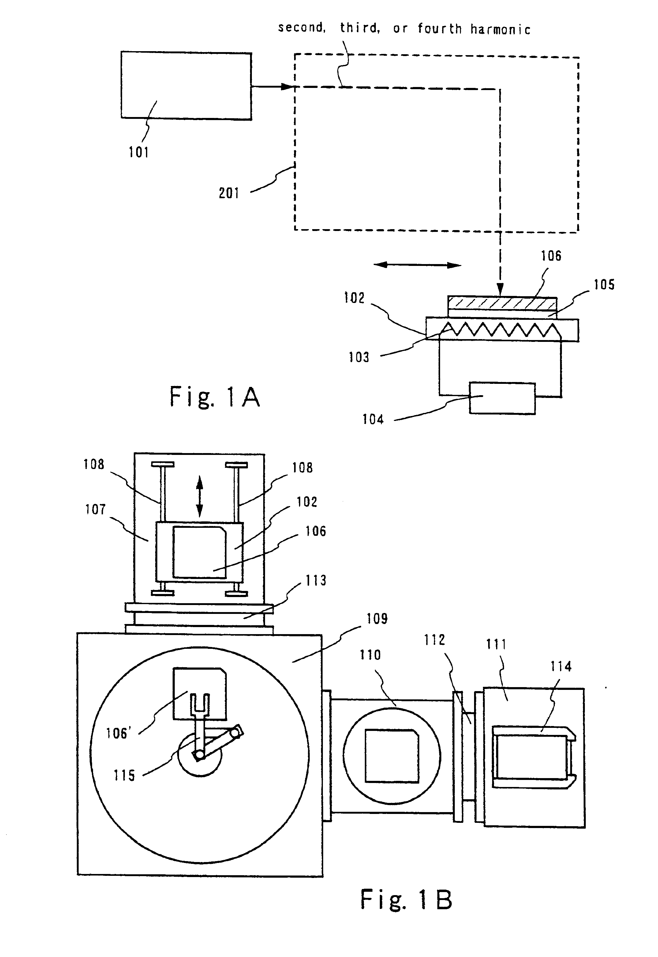
[0042]An embodiment mode of the present invention will be described. FIG. 1A is a diagram showing the structure of an laser apparatus including a laser of the present invention. This laser apparatus has an Nd: YAG laser 101, an optical system 201 for linearizing laser light (preferably second harmonic, third harmonic, or fourth harmonic) generated and emitted from an Nd:YAG laser 101, and a stage 102 on which a light transmittable substrate is fixed. The stage 102 is provided with a heater 103 and a heater controller 104 to heat the substrate up to a temperature of 100 to 450° C. A reflective member 105 is provided on the stage 102, and placed on the reflective member 105 is a substrate 106 on which an amorphous semiconductor film is formed.

[0043]If the laser light output from the Nd:YAG laser 101 is modulated into any of the second to fourth harmonics, a wavelength modulator including a non-linear element is set right behind the Nd:YAG laser 101.

[0044]Next will be described, with r...

embodiment mode 2

[0061]A description given here is a different mode for carrying out the present invention from Embodiment Mode 1. This embodiment mode shows an example in which, without using a reflecting member as described in Embodiment Mode 1, an amorphous semiconductor film is irradiated from its front and back with laser light split into two strains of laser light by some constituent of an optical system.

[0062]FIG. 4A is a diagram showing the structure of a laser apparatus including a laser of this embodiment mode. The structure is basically the same as that of the laser apparatus described in Embodiment Mode 1 with FIGS. 1A and 1B. Accordingly, only parts different from the ones in the precedent mode are given different symbols and are explained.

[0063]This laser apparatus has an Nd: YAG laser 101, an optical system 401 for linearizing laser light that is generated and emitted from an Nd:YAG laser 101 and splitting into two strains laser light (preferably third harmonic, or fourth harmonic), a...

embodiment mode 3

[0073]A description given here is about an embodiment mode different from Embodiment Mode 2. This embodiment mode shows an example in which laser light is split into two strains of laser light by some constituent of an optical system, the two laser beams are made into a third harmonic and a fourth harmonic, respectively, and laser annealing of an amorphous semiconductor film is carried out by irradiating its front with the fourth harmonic while irradiating its back with the third harmonic.

[0074]FIG. 6 is a side view of the optical system of a laser apparatus for use in this embodiment mode. The laser light generated and emitted from an Nd:YAG laser 601 as a source is split by a half mirror 602. Note that, though not shown, a part of a fundamental wave output from the Nd:YAG laser 601 is modulated into a third harmonic having a wavelength of 335 nm before reaching the half mirror 602.

[0075]First, laser light which has transmitted through the half mirror 602 (to serve as a secondary l...


PUM


Abstract

To provide a laser apparatus and a laser annealing method with which a crystalline semiconductor film with a larger crystal grain size is obtained and which are low in their running cost. A solid state laser easy to maintenance and high in durability is used as a laser, and laser light emitted therefrom is linearized to increase the throughput and to reduce the production cost as a whole. Further, both the front side and the back side of an amorphous semiconductor film is irradiated with such laser light to obtain the crystalline semiconductor film with a larger crystal grain size.

Description

BACKGROUND OF THE INVENTION[0001]1. Field of the Invention[0002]The present invention relates to a method of annealing a semiconductor film with the use of laser light (hereinafter referred to as laser annealing) and to a laser apparatus for performing the laser annealing (an apparatus including a laser and an optical system for leading laser light output from the laser to a process object). The invention also relates to a semiconductor device fabricated by a manufacturing process that comprises the laser annealing step, and to the manufacturing process. The semiconductor device here includes an electro-optical device such as a liquid crystal display device and an EL display device, and an electronic device having the electro-optical device as one of its components.[0003]2. Description of the Related Art[0004]An advance has been made in recent years in development of thin film transistors (hereinafter referred to as TFTs), and TFTs using polycrystalline silicon films (polysilicon fi...

Claims


Application Information

Patent Timeline
Patent Type & Authority Patents(United States)
IPC IPC(8): H01L21/20
CPCH01L21/2026H01L27/1285Y10S438/904H01L21/02691H01L21/02683H01L21/02532H01L21/02488H01L21/02422H01L21/02595
Inventor YAMAZAKI, SHUNPEIOHTANI, HISASHITANAKA, KOICHIROKASAHARA, KENJIKAWASAKI, RITSUKO
Owner SEMICON ENERGY LAB CO LTD
Why Eureka
Try Eureka