Method of enhancing laser crystallization for polycrystalline silicon fabrication

a technology of laser crystallization and polycrystalline silicon, which is applied in the direction of basic electric elements, electrical apparatus, and semiconductor devices, can solve the problems of limited electrical characteristics of polycrystalline silicon thin film, inapplicable high-performance flat panel displays, and significant influence on the device performance of polycrystalline silicon tfts such as carrier mobility, so as to enhance the growth of amorphous silicon crystallization, improve laser crystallization effect, and improve the effect of laser energy utilization

Inactive Publication Date: 2006-04-27
IND TECH RES INST
View PDF8 Cites 25 Cited by
  • Summary
  • Abstract
  • Description
  • Claims
  • Application Information

AI Technical Summary

Benefits of technology

[0014] With the application of the present invention, grain growth of amorphous silicon crystallization is enhanced by an additional heating function from the heat-retaining layer, and the laser energy density used in the laser irradiation process to effect the melting of the amorphous silicon layer is reduced by the anti-reflective thickness design of the heat-retaining layer. Therefore, a laser crystallization effect is improved greatly to obtain polycrystalline silicon with large grains in a general laser irradiation process. Besides, the laser energy is utilized more effectively. Moreover, laser energy distribution absorbed in the amorphous silicon layer is more uniform because of the heat-retaining layer formation, and a frequently repeated laser operation in the conventional laser process is thus avoided. A single shot laser is sufficient to achieve a good ...

Problems solved by technology

However, the device performance of polycrystalline silicon TFTs, such as carrier mobility, is significantly affected by the crystal grain size.
Those techniques are not applicable to high performance flat panel displays because the crystalline quality is limited by the low process temperature (typically lower than 650° C.
Hence, the electrical characteristics of polycrystalline silicon thin film are limited.
However, this value is yet not sufficient for future demand of high performance flat panel displays.
Besides, unstabl...

Method used


Image

  • Method of enhancing laser crystallization for polycrystalline silicon fabrication
  • Method of enhancing laser crystallization for polycrystalline silicon fabrication
  • Method of enhancing laser crystallization for polycrystalline silicon fabrication

Examples


embodiment 1

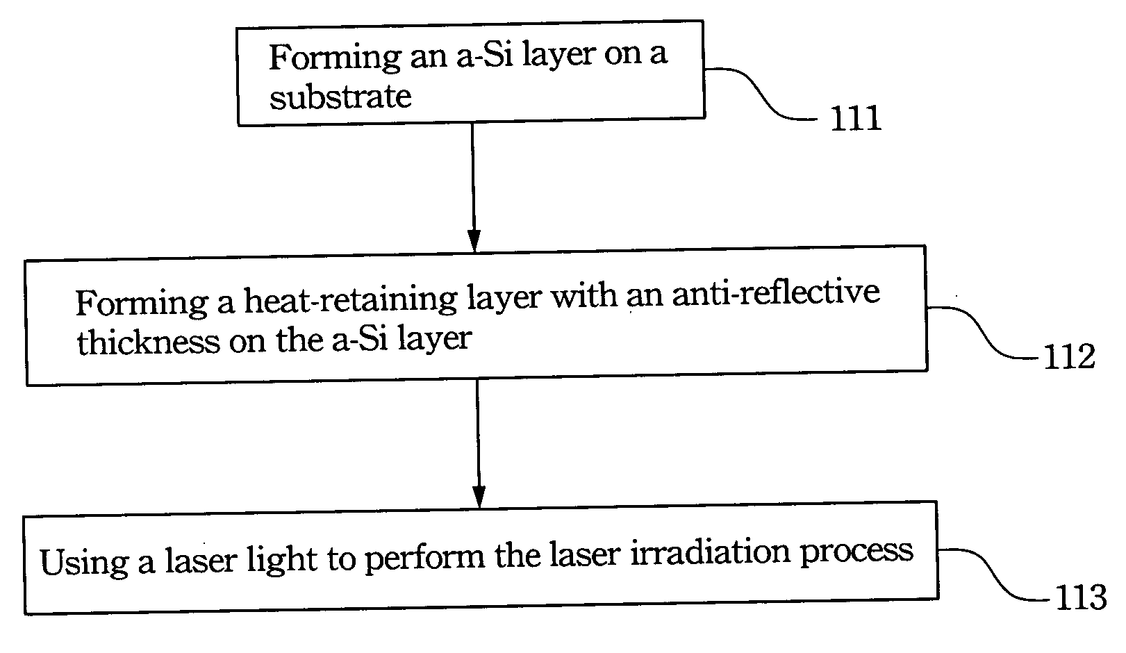
[0024] The present invention discloses a method of enhancing laser crystallization for polycrystalline silicon fabrication. A semitransparent material is used as the heat-retaining layer capped on the amorphous silicon layer to lengthen the amorphous silicon melting time in a laser irradiation process. When the laser irradiation process is performed, a portion of the laser energy passes through the heat-retaining layer to effect the melting of the amorphous silicon layer, while another portion is absorbed by the heat-retaining layer to continuously heat the melted amorphous silicon layer and hence lengthen the cooling time of melted amorphous silicon. Crystallization of the amorphous silicon layer is thus improved to further enhance grain growth for forming a high quality polycrystalline silicon layer with large grains.

[0025] However, the heat-retaining layer is not only semitransparent, but reflects incident laser light in general, so the laser energy used cannot be transmitted to...

embodiment 2

[0036] The present invention discloses another method of enhancing laser crystallization for polycrystalline silicon fabrication. Two heat-retaining layers are utilized to cap the amorphous silicon layer. Besides, anti-reflectivity to laser light is obtained by controlling the anti-reflective thickness of the two heat-retaining layers, and the two heat-retaining layers have a dielectric capability by choosing a suitable material as the heat-retaining layers for TFT device fabrication.

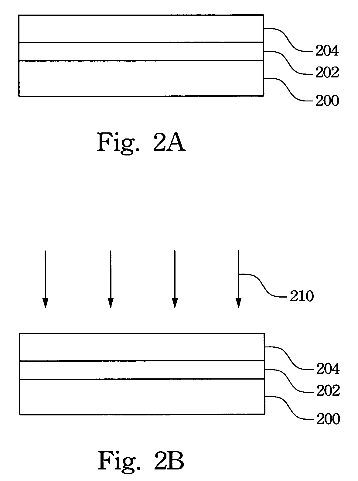
[0037] Referring to FIGS. 4A-4B, FIGS. 4A-4B are cross-sectional schematic diagrams showing the process for enhancing laser crystallization in accordance with the second preferred embodiment of the present invention. First, referring to FIG. 4A, an amorphous silicon layer 402 is formed on a substrate 400 by, for example, PECVD or PVD, and dehydrogenation is then performed on the amorphous silicon layer 402 to prevent a hydrogen explosion during the subsequent laser annealing.

[0038] Then, a first heat-...


PUM


Abstract

An amorphous silicon layer and at least a heat-retaining layer are formed on a substrate in turn. Wherein, the heat-retaining layer is controlled to have an anti-reflective thickness for reducing the threshold laser energy to effect the melting of the amorphous silicon layer. Then, a laser irradiation process is performed to transform the amorphous silicon layer into a polycrystalline silicon layer. During the laser irratiation process, a portion of the laser energy transmits the heat-retaining layer to effect the melting of the amorphous silicon layer, and another portion of the laser energy is absorbed by the heat-retaining layer.

Description

RELATED APPLICATIONS [0001] The present application is based on, and claims priority from, Taiwan Application Serial Number 93132223, filed Oct. 22, 2004, the disclosure of which is hereby incorporated by reference herein in its entirety. FIELD OF THE INVENTION [0002] The present invention relates to a method of enhancing laser crystallization, and more particularly, to a method of enhancing laser crystallization by a heat-retaining layer with an anti-reflectivity function for polycrystalline silicon fabrication. BACKGROUND OF THE INVENTION [0003] Polycrystalline silicon thin film as a high quality active layer in semiconductordevices has lately attracted considerable attention due to its superior charge carrier transport property; and high compatibility with current semiconductor device fabrication. With low temperature process, it is possible to fabricate reliable polycrystalline silicon thin film transistors (TFTs) on transparent glass or plastic substrates for making polycrystal...

Claims


Application Information

Patent Timeline
IPC IPC(8): H01L21/20
CPCH01L21/2026H01L27/1281H01L29/66757H01L21/02686H01L21/02422H01L21/02532H01L21/02595
Inventor LIN, JIA-XINGCHEN, CHI-LINCHEN, YU-CHENGTSAI, PO-HAO
Owner IND TECH RES INST
Why Eureka
Try Eureka