Display device and method of manufacturing the same

a technology of display device and manufacturing method, which is applied in the direction of instruments, non-linear optics, optics, etc., can solve the problems of reducing the yield, reduce the contact resistance, reduce the sheet resistance of the peripheral portion and prevent the disconnection of the storage capacitor electrode due to the step of the opening

Active Publication Date: 2011-12-06
JAPAN DISPLAY WEST
View PDF26 Cites 25 Cited by
  • Summary
  • Abstract
  • Description
  • Claims
  • Application Information

AI Technical Summary

Benefits of technology

[0014]With this structure, since the storage capacitor electrode is made of microcrystalline polysilicon and the flatness of the surface is enhanced, dielectric strength between the storage capacitor electrode and the upper storage capacitor electrode is enhanced.
[0016]With this structure, the pattern of the storage capacitor electrode is formed larger than the bottom portion of the opening, the edge of the peripheral portion of the storage capacitor electrode is located on the buffer film on the slant portion of the opening or the buffer film on the outside of the opening, and the crystal grain size of the peripheral portion of the storage capacitor electrode is larger than that on the inner side from the peripheral portion. Therefore, the sheet resistance of the peripheral portion of the storage capacitor electrode is reduced, thereby achieving reduction of the contact resistance between the thin film transistor and the storage capacitor. Furthermore, disconnection of the storage capacitor electrode due to the step of the opening is prevented.

Problems solved by technology

This increases contact resistance between the thin film transistor and the storage capacitor, and the yield may reduce.

Method used


Image

  • Display device and method of manufacturing the same
  • Display device and method of manufacturing the same
  • Display device and method of manufacturing the same

Examples


Embodiment Construction

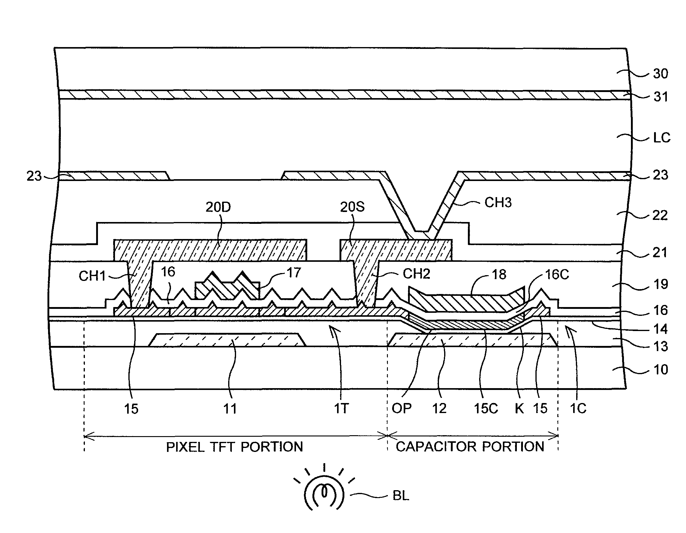
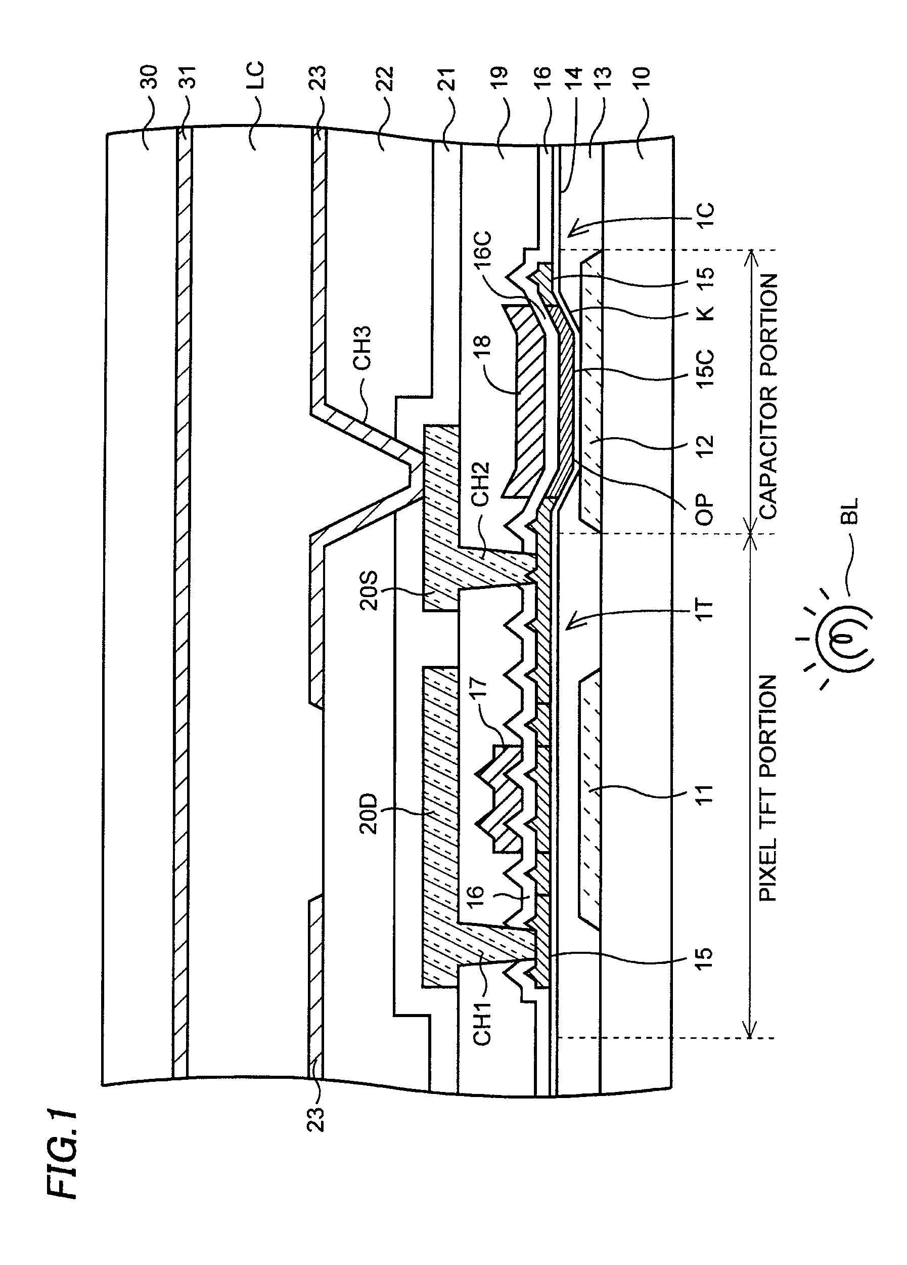
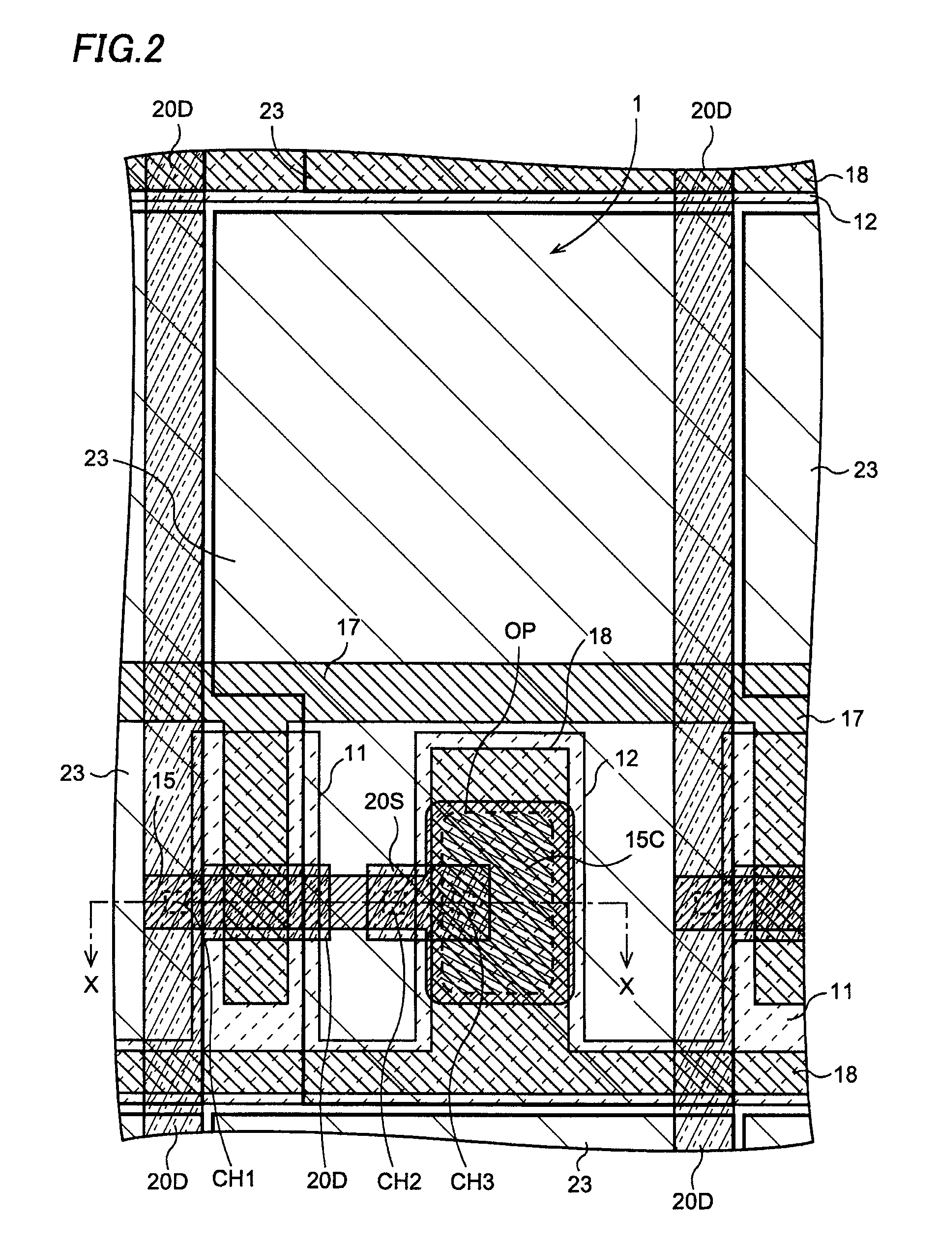
[0023]A display device and a method of manufacturing the display device of an embodiment of the invention will be described referring to figures. Although a plurality of pixels is formed in this display device, FIG. 1 shows one pixel 1. A cross-sectional structure on a first substrate 10 side shown in FIG. 1 corresponds to a cross-section of a plan view of FIG. 2 along line X-X. The same numerals are given to the same components in FIG. 1 and FIG. 2 as those shown in FIG. 5.

[0024]The first substrate 10 made of a transparent insulation material such as glass includes a pixel TFT portion where a pixel TFT 1T is formed and a capacitor portion where a storage capacitor 1C is formed. First, a light-shielding metal layer 11 made of molybdenum, chromium or the like and blocking external light incident on the first substrate 10 is formed on the first substrate 10 in the pixel TFT portion. A lower storage capacitor electrode 12 is formed on the first substrate 10 in the capacitor portion. Th...


PUM


Abstract

The invention provides a display device having a thin film transistor and a storage capacitor storing a display signal applied to a pixel electrode through this thin film transistor on a substrate, where dielectric strength between electrodes forming the storage capacitor is enhanced for increasing the yield. In the storage capacitor, a lower storage capacitor electrode, a thin lower storage capacitor film, a polysilicon layer, an upper storage capacitor film and an upper storage capacitor electrode are layered. The polysilicon layer is formed by crystallization by laser annealing. The polysilicon layer of the storage capacitor is microcrystalline and thus the flatness of its surface is enhanced. The pattern of the polysilicon layer (storage capacitor electrode) is formed larger than the bottom portion of an opening, and the edge of its peripheral portion is located on a buffer film on the slant portion of the opening or on the buffer film on the outside of the opening.

Description

CROSS-REFERENCE OF THE INVENTION[0001]This invention claims priority from Japanese Patent Applications Nos. 2006-249670, 2006-249671 and 2007-179898, the contents of which are incorporated herein by reference in these entirety.BACKGROUND OF THE INVENTION[0002]1. Field of the Invention[0003]The invention relates to a display device having a thin film transistor and a storage capacitor storing a display signal applied to a pixel electrode through this thin film transistor on a substrate and a method of manufacturing the same.[0004]2. Description of the Related Art[0005]An active matrix type liquid crystal display device has a pixel selecting thin film transistor (hereafter, referred to as a “pixel TFT”) in each of a plurality of pixels disposed into a matrix on a glass substrate. It also has a storage capacitor formed for storing a display signal applied to a pixel electrode through the pixel TFT.[0006]This liquid crystal display device and a method of manufacturing the device will be...

Claims


Application Information

Patent Timeline
Patent Type & Authority Patents(United States)
IPC IPC(8): H01L29/04
CPCG02F1/136213H01L29/04H01L27/1281H01L27/1255H01L29/78633H01L27/1214H01L27/13
Inventor SAKURAI, TORUMORIMOTO, YUSAKUUMETANI, YUTAKA
Owner JAPAN DISPLAY WEST
Why Eureka
Try Eureka