Method for forming semiconductor device and method for forming photovoltaic device

Inactive Publication Date: 2008-04-24
CANON KK
View PDF12 Cites 26 Cited by
  • Summary
  • Abstract
  • Description
  • Claims
  • Application Information

AI Technical Summary

Benefits of technology

[0042] The present invention is intended to solve the above problems and to readily optimize the conditions where a microcrystalline silicon film (one type of silicon film containing crystals) is formed. An object of the present invention is to provide a microcrystalline silicon fi

Problems solved by technology

Accordingly, the development of techniques for increasing the deposition rate in high-frequency plasma-enhanced CVD and achieving a further improvement in characteristics is an important technological issue.
However, some problems must be solved to further improve the characteristics of photovoltaic devices including silicon deposited films containing crystals, and to reduce their costs.
A first problem is (1) induction of sparks that destabilize plasma and (2) increased growth of fine particles of byproducts such as polysilane in the plasma, depending on the conditions where the deposited film is formed.
The sparks adversely affect the characteristics of the deposited film because they increase, for example, structural defects in the deposited film.
If a spark occurs on the surface of the deposited film, the spark itself damages the surface of the deposited film, thus forming a structural defect.
Such an interface can adversely affect, for example, the electrical or optical characteristics of the deposited film.
Sparks with longer durations have a larger adverse effect on the deposited film.
However, extremely small sparks (with spark durations of several microseconds to several tens of milliseconds) have not been understood in detail because they are difficult to visually recognize and the discharge remains apparently stable.
A spark killer (a device that detects a change in bias current and reduces or interrupts the voltage being applied upon detection of a predetermined value of current) is known for use as a spark-suppressing device, but sparks are difficult to completely avoid.
For example, if the sensitivity of the spark killer is increased, the bias voltage is frequently interrupted due to noise other than sparks.
This makes it difficult to perform stable discharge.
Accordingly, while spark killers are intended to suppress the frequency of occurrence or magnitude of sparks, they cannot always sufficiently suppress the occurrence of small sparks.
As described above, optimizing the conditions where a deposited film is formed is not easy because the occurrence of sparks and fine particles of, for example, polysilane can be induced.
A secon

Method used


Image

  • Method for forming semiconductor device and method for forming photovoltaic device
  • Method for forming semiconductor device and method for forming photovoltaic device
  • Method for forming semiconductor device and method for forming photovoltaic device

Examples


Example

Example 1

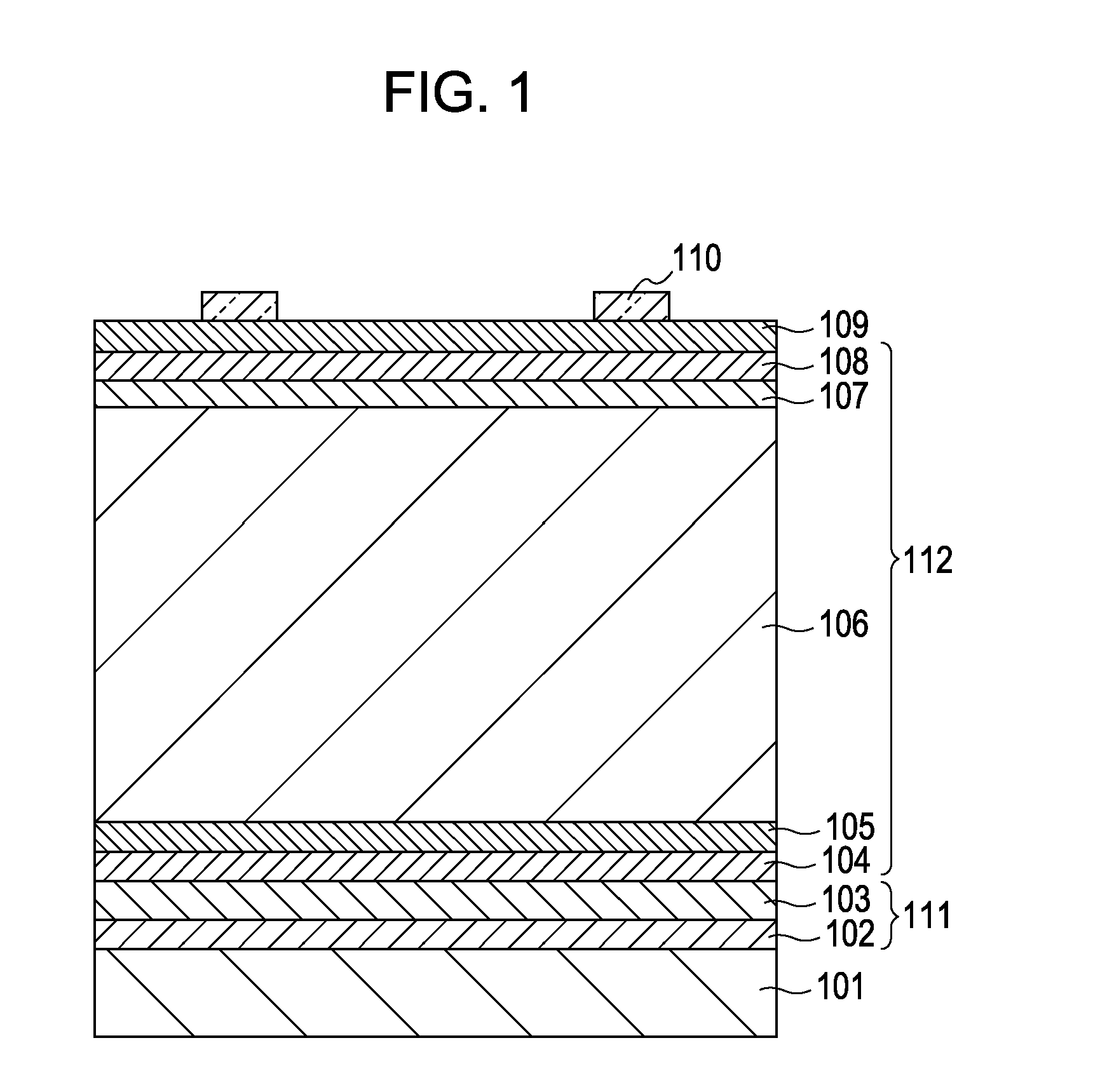
[0252] A strip-like stainless (SUS430BA) substrate (width: 40 cm; length: 200 m; thickness: 0.125 mm) is sufficiently degreased and cleaned and is inserted into a continuous sputtering apparatus (not shown). A silver film is deposited to a thickness of 100 nm on the substrate by sputtering using a silver electrode as a target. A ZnO film is then deposited to a thickness of 1.2 μm on the silver film by sputtering using a ZnO target. Thus, a strip-like conductive substrate is prepared.

[0253] Next, n-type, i-type, and p-type semiconductor layers are sequentially deposited on the substrate by the procedure described above under the conditions shown in Table 1. An ITO transparent conductive film is deposited to a thickness of 80 nm on each n-i-p photoelectric conversion unit as a front electrode by sputtering using a sputtering apparatus (not shown). An interdigital silver electrode for outputting current is then deposited on the transparent conductive film by vapor deposition...

Example

Example 2

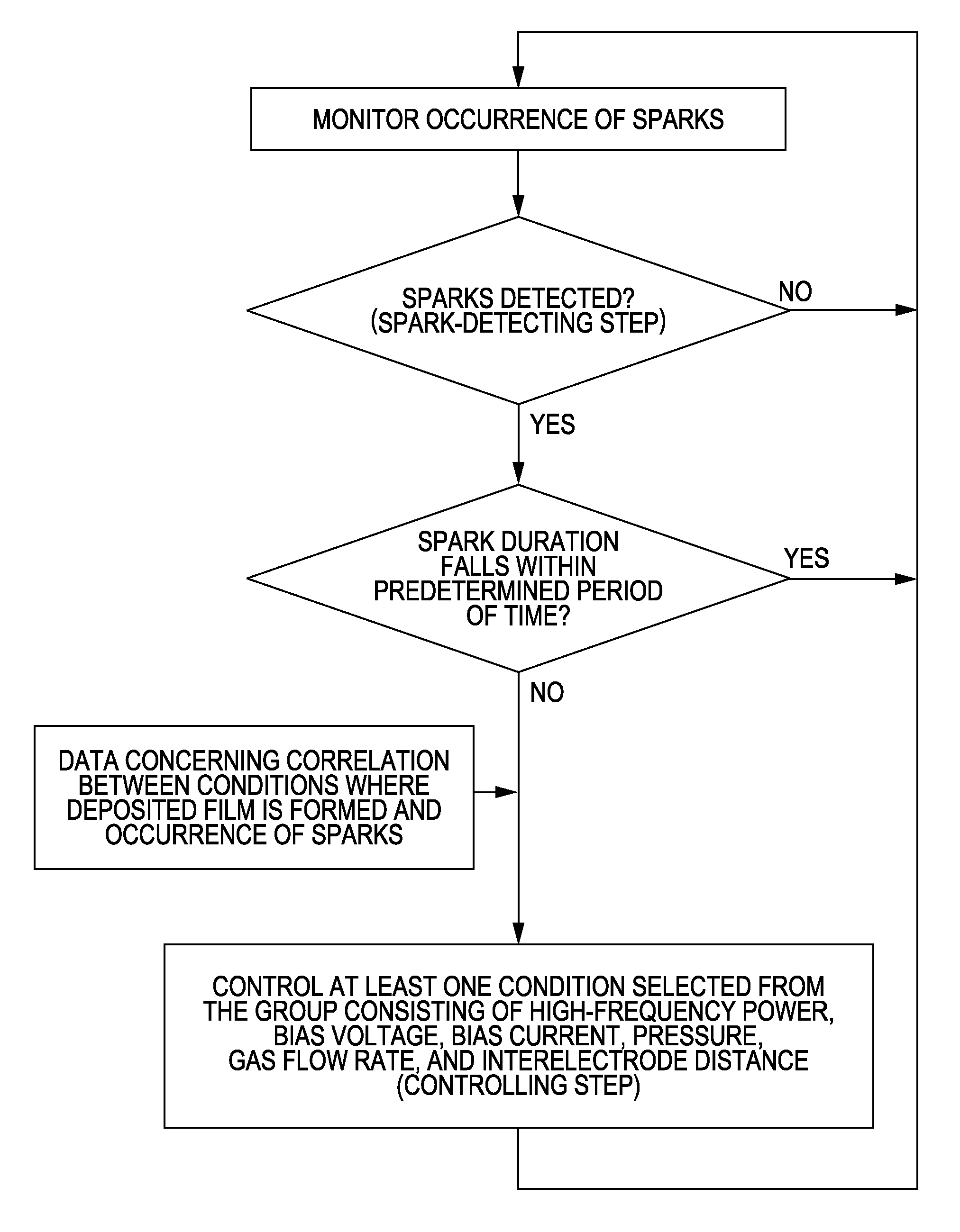
[0282] Samples are produced under the same conditions as in Example 1 except that the deposition pressure and the gas flow rate at which the i-type layer, the p / i buffer layer, and the n / i buffer layer are deposited are changed on the basis of the results of the preliminary experiment so that the number of sparks with durations of 100 ms or more is substantially 0 sparks and the number of sparks with durations of 50 μs to 20 ms is 5 or less sparks per minute. These samples are evaluated as in Example 1.

[0283] The results are shown in Table 2 together with the results of Example 1.

Example

Example 3

[0284] Samples are produced under the same conditions as in Example 1 except that the deposition pressure and the gas flow rate at which the i-type layer, the p / i buffer layer, and the n / i buffer layer are deposited are changed on the basis of the results of the preliminary experiment so that the number of sparks with durations of 100 ms or more is substantially 0 sparks and the number of sparks with durations of 20 to 100 ms is 3 or less sparks per minute. These samples are evaluated as in Example 1.

[0285] The results are shown in Table 2 together with the results of Example 1.


PUM

PropertyMeasurementUnit
Lengthaaaaaaaaaa
Timeaaaaaaaaaa
Thicknessaaaaaaaaaa

Abstract

A method for forming a semiconductor device including a semiconductor layer, formed of a silicon-based deposited film containing crystals by plasma-enhanced CVD, includes the steps of applying a bias voltage between a high-frequency electrode and a substrate with the high-frequency electrode being negative when the semiconductor layer is formed; detecting sparks occurring on the high-frequency electrode or the substrate; and controlling at least one condition, selected from the group consisting of high-frequency power, bias voltage, bias current, pressure, gas flow rate, and interelectrode distance, based on the results of the detection so that the number of sparks with durations of 100 ms or more is 1 or less sparks per minute.

Description

BACKGROUND OF THE INVENTION [0001] 1. Field of the Invention [0002] The present invention relates to methods for forming semiconductor devices including deposited films, particularly, silicon-based deposited films, and methods for forming photovoltaic devices, such as solar cells, including silicon-based deposited films. [0003] 2. Description of the Related Art [0004] High-frequency plasma-enhanced chemical vapor deposition (CVD) is one superior method for mass production of silicon-based deposited films because this method facilitates formation of large films at low temperature with high process throughput. Examples of applications of such silicon-based deposited films for products include solar cells. In comparison with existing energy generation systems using fossil fuels, solar cells including silicon-based deposited films have the advantage of using an infinite energy source and a clean power generation process. However, a further cost reduction is required to promote widesprea...

Claims


Application Information

Patent Timeline
IPC IPC(8): H01L21/00
CPCC23C16/24C23C16/4401C23C16/509Y02E10/545H01L21/67253H01L31/1824C23C16/545Y02P70/50
Inventor TAKAI, YASUYOSHISAWAYAMA, TADASHIMORIYAMA, KOICHIRO
Owner CANON KK
Why Eureka
Try Eureka