Conductive sintered layer forming composition and conductive coating film forming method and bonding method using the same

a technology of coating film and conductive sintered layer, which is applied in the direction of oxide conductors, non-metal conductors, semiconductor/solid-state device details, etc., can solve the problems of large volume contraction, low heating temperature, and large number of voids in junction layers, so as to shorten heating time and reduce heating temperature

Inactive Publication Date: 2008-07-03
HITACHI LTD
View PDF6 Cites 123 Cited by
  • Summary
  • Abstract
  • Description
  • Claims
  • Application Information

AI Technical Summary

Benefits of technology

[0013]Thus, the invention can provide the conductive sintered layer forming composition and the conductive sintered layer forming method that allow the lowering of heating...

Problems solved by technology

However, because it is necessary to reduce thermal damage (e.g., when applied to organic substrate whose heat resistance is low) and thermal deformation such as warp of peripheral members in the process described above, it is required to lower heating temperature.
However, there ha...

Method used


Image

  • Conductive sintered layer forming composition and conductive coating film forming method and bonding method using the same
  • Conductive sintered layer forming composition and conductive coating film forming method and bonding method using the same
  • Conductive sintered layer forming composition and conductive coating film forming method and bonding method using the same

Examples


first embodiment

[0057]The invention utilizes the conductive sintered layer forming composition using the phenomenon that it is possible to sinter at low temperature as compared to sintering each simple substance, by mixing metal particles coated with the organic substance, with silver oxide.

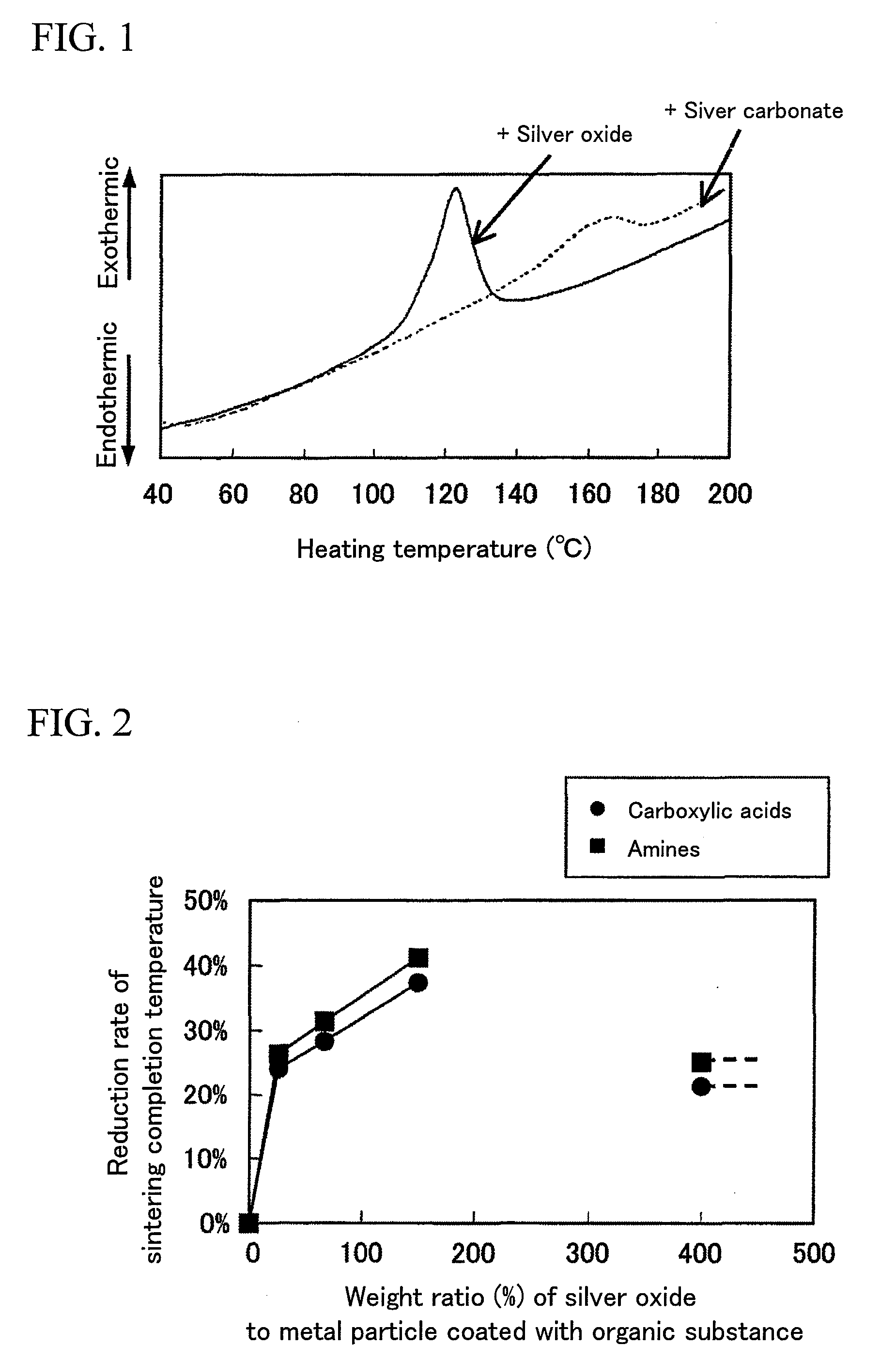
[0058]In order to confirm this phenomenon, the effect obtained by mixing the silver oxide particles with the metal particles coated with the organic substance has been studied in the first embodiment. The silver oxide particles having an average grain size of about 2 μm and silver nano-particles having a grain size of 1 to 100 nm are used while using carboxylic acids as the organic substance for coating the metal particles. FIG. 1 shows results of a thermal analysis of the composition in which silver oxide is mixed in terms of weight ratio of 100 to the silver nano-particles coated with the carboxylic acids. The thermal measurement has been carried out in an atmosphere by using TG / DTA6200 manufactured by Seiko I...

second embodiment

[0060]The conductive sintered layer may be fabricated at low processing temperature by using the conductive sintered layer forming composition of the invention. FIG. 2 is a graph showing a temperature lowering rate of the process completion temperature to a case when a simple substance of the metal particle coated with the organic substance is used. The silver nano-particles having a grain size of 1 to 100 nm and coated with carboxylic acids and the silver nano-particles having a grain size of 1 to 1000 nm and coated with amines have been used as the metal particles coated with the organic substance, and silver oxide particles having an average grain size of about 2 μm are mixed with each of them so as to be in the weight ratio represented by an axis of abscissa in FIG. 2. Only the temperature raising process has been given as the heating process with heating speed of 10° C. / min. in order to eliminate an influence of holding time in the heating process. The process has been finished...

third embodiment

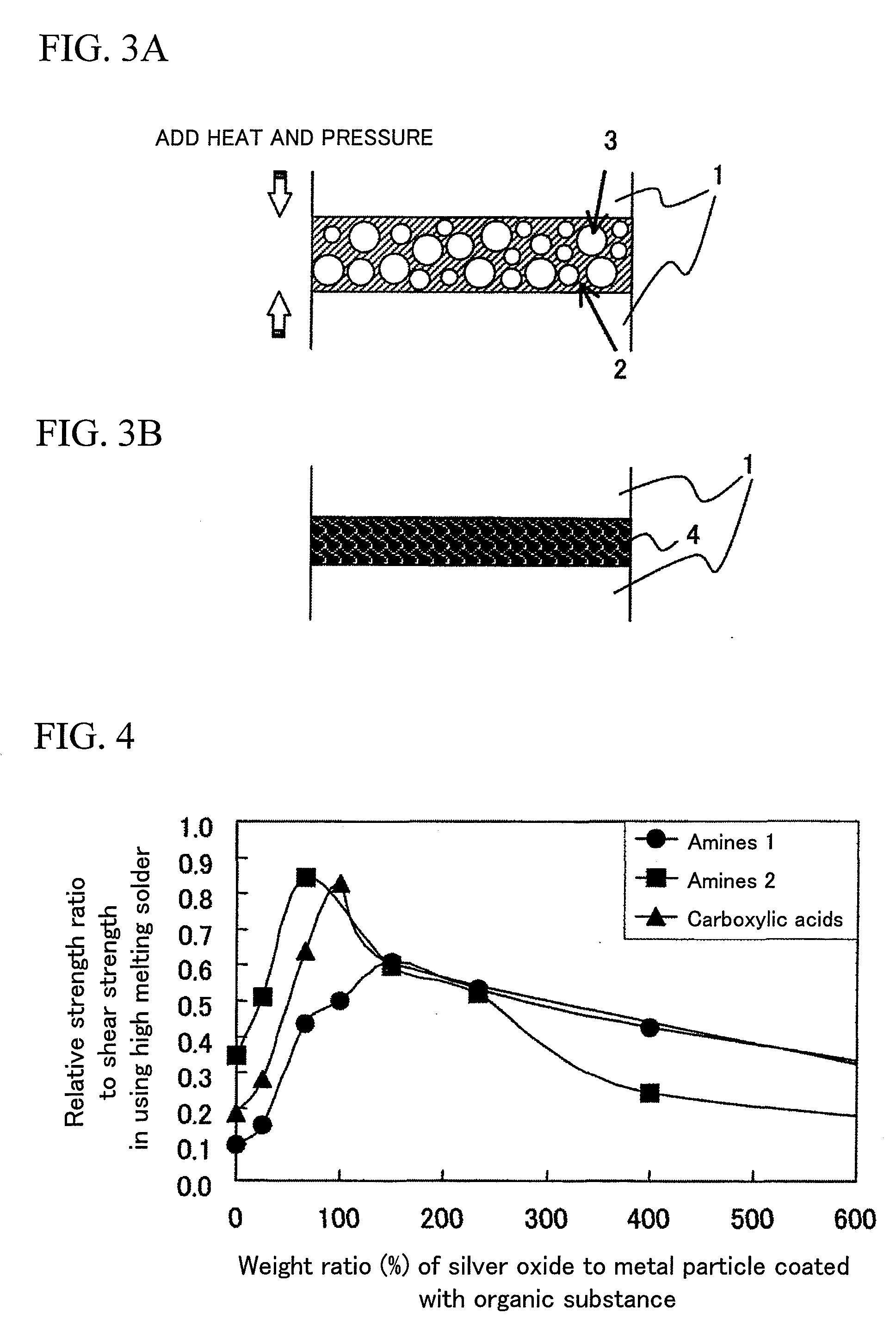
[0063]A point that it becomes possible to obtain high bonding strength at low temperature by using the conductive sintered layer forming composition of the invention as a bonding material as compared to a case of using the simple substance of the metal particles coated with the organic substance will be explained below.

[0064]The silver nano-particles having a grain size of 1 to 100 nm and coated with carboxylic acids, the silver nano-particles having a grain size of 1 to 10 nm and coated with amines and the silver nano-particles having a grain size of 1 to 1000 nm and coated with amines have been used as the metal particles coated with the organic substance. Then, the conductive sintered layer forming composition of the invention was obtained by mixing silver oxide particles having an average grain size of about 2 μm with the respective silver nano-particles so that the content of silver oxide within the composition becomes as indicated by the weight ratio represented by an axis of ...


PUM

PropertyMeasurementUnit
Grain sizeaaaaaaaaaa

Abstract

There is provided a conductive sintered layer forming composition and a conductive sintered layer forming method that can lower heating temperature and shorten heating time for a process of accelerating sintering or bonding by sintering of metal nano-particles coated with an organic substance. The conductive sintered layer forming composition may be obtained by utilizing a phenomenon that particles may be sintered at low temperature by mixing silver oxide with metal particles coated with the organic substance and having a grain size of 1 nm to 5 μm as compared to sintering each simple substance. The conductive sintered layer forming composition of the invention is characterized in that it contains the metal particles whose surface is coated with the organic substance and whose grain size is 1 nm to 5 μm and the silver oxide particles.

Description

BACKGROUND OF THE INVENTION[0001]1. Field of the Invention[0002]The present invention to a conductive sintered layer forming composition applicable for use in bonding in packaging electronic parts and semiconductors to a circuit board or a lead frame or in forming a conductive film such as wires and electrodes and a conductive coating film forming method using the same.[0003]2. Related Art[0004]It has been known that when a grain size of a metal particle decreases to nano-size and a number of structuring atoms decreases, a ratio of a surface area to a volume of the particle increases sharply and melting point and sintering temperature drop remarkably as compared to a bulk state (particles whose grain size is 1 to 1000 nm will be defined as a nano-particle in the present specification). Then, it has been reported to apply the nano-particle as a component or a bonding material in forming a conductive coating film or wires by utilizing the low temperature sintering function of the nano...

Claims


Application Information

Patent Timeline
IPC IPC(8): H01B1/08B05D5/12B22F7/04C09C1/62C09C3/08C09D5/24C09D7/12C09D11/00C09D11/52C09D201/00H01B1/00H01B1/22H01B13/00H01L21/52H01R11/01H05K1/09H05K3/32
CPCB22F7/04H01B1/08H01L23/3735H01L23/3737H01L24/29H01L24/33H01L24/40H01L24/83H01L24/91H01L2224/29339H01L2224/29344H01L2224/29355H01L2224/29364H01L2224/29366H01L2224/29369H01L2224/32225H01L2224/32245H01L2224/45015H01L2224/45124H01L2224/48247H01L2224/49175H01L2224/73221H01L2224/83801H01L2224/8384H01L2924/01005H01L2924/01013H01L2924/01014H01L2924/01029H01L2924/01046H01L2924/01047H01L2924/0105H01L2924/01074H01L2924/01078H01L2924/01079H01L2924/01082H01L2924/09701H01L2924/10253H01L2924/13091H01L2924/15153H01L2924/15165H01L2924/19041H01L2924/19043H01L2924/19105H01L2924/2076H05K1/097H05K3/321H05K2201/0224H01L24/48H01L2224/2919H01L2224/73265H01L2924/01006H01L2924/01019H01L2924/01033H01L2924/014H01L2924/0665H01L2224/29101H01L24/49H01L2224/29111H01L2924/0132H01L2924/0133H01L2224/8584H01L2224/45139H01L2224/45147H01L2924/15787H01B1/02H01L2224/29139H01L2924/01028H01L2224/27334H01L2924/00014H01L2924/00H01L2924/3512H01L2924/181H01L2224/40225H01L2224/85205H01L2924/00011H01L2924/12042H01L24/45H01L2924/19107H01L2224/8484H01L24/37H01L2224/37147H01L24/84H01L2224/83205H01L2924/00012H01L2924/01049
Inventor IDE, EIICHIMORITA, TOSHIAKIYASUDA, YUSUKEHOZOJI, HIROSHI
Owner HITACHI LTD
Why Eureka
Try Eureka