Silicon carbide substrate, epitaxial layer provided substrate, semiconductor device, and method for manufacturing silicon carbide substrate

a technology of silicon carbide and epitaxial layer, which is applied in the direction of semiconductor devices, electrical devices, basic electric elements, etc., can solve the problems of reducing the on-resistance of the semiconductor device, and achieve the effect of reducing the on-resistan

Inactive Publication Date: 2012-05-17
SUMITOMO ELECTRIC IND LTD
View PDF3 Cites 121 Cited by
  • Summary
  • Abstract
  • Description
  • Claims
  • Application Information

AI Technical Summary

Benefits of technology

[0015]Thus, the present invention can provide a silicon carbide substrate, an epitaxial layer provided substrate, a semiconductor device, and a method for manufacturing the silicon carbide substrate, each of which achieves reduced on-resistance.

Problems solved by technology

The documents described above achieve a low-resistant ohmic contact in the silicon carbide substrate, which results in reduced on-resistance of the semiconductor device.

Method used


Image

  • Silicon carbide substrate, epitaxial layer provided substrate, semiconductor device, and method for manufacturing silicon carbide substrate
  • Silicon carbide substrate, epitaxial layer provided substrate, semiconductor device, and method for manufacturing silicon carbide substrate
  • Silicon carbide substrate, epitaxial layer provided substrate, semiconductor device, and method for manufacturing silicon carbide substrate

Examples


first embodiment

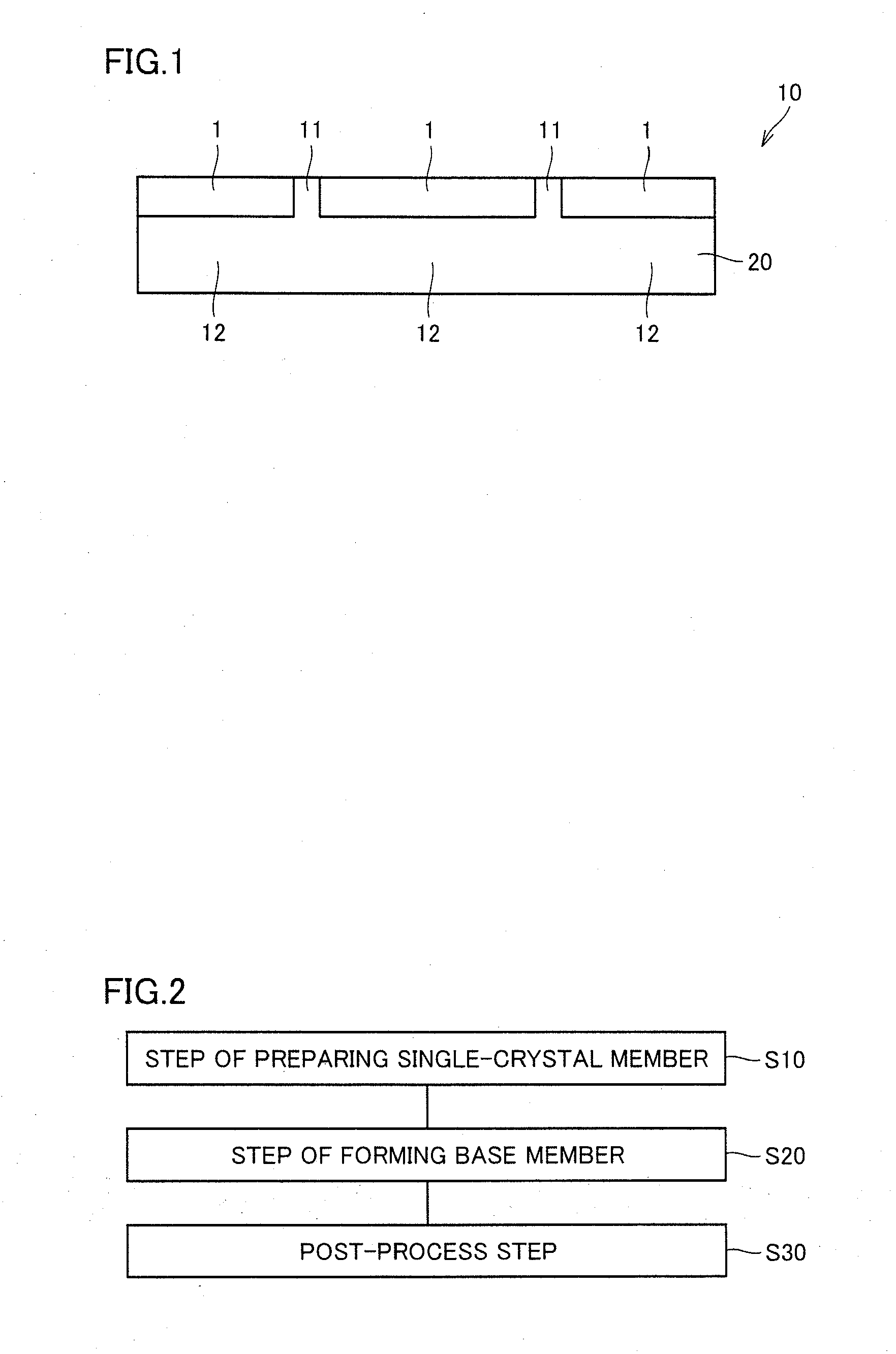
[0039]Referring to FIG. 1, a silicon carbide substrate of a first embodiment according to the present invention will be described.

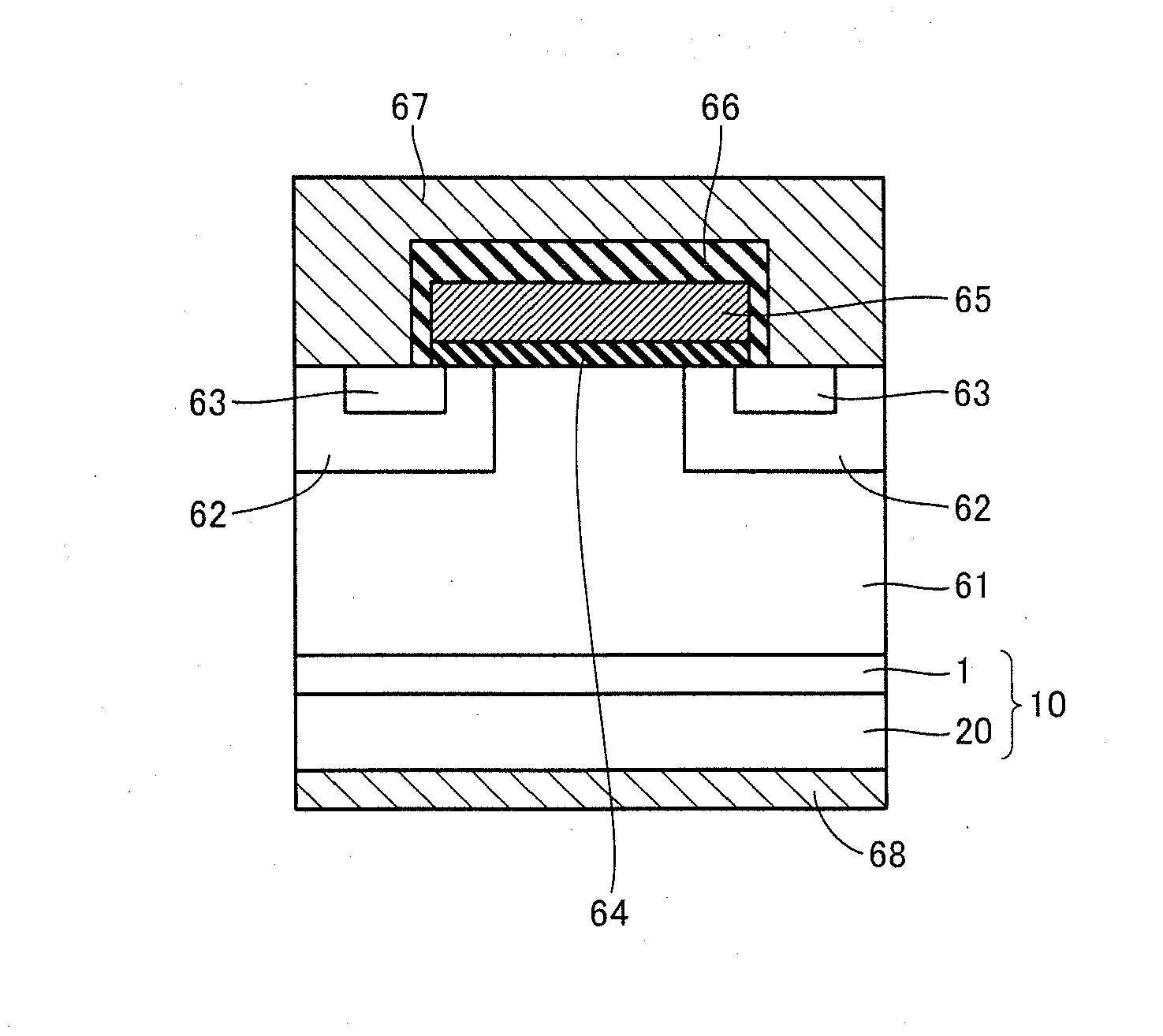
[0040]As shown in FIG. 1, a silicon carbide substrate 10 according to the present invention is a composite substrate including SiC single-crystal substrates 1 each serving as a single-crystal member, and a base member 20 serving as a supporting base. Silicon carbide substrate 10, which has a circular planar shape, has one main surface in which the plurality of SiC single-crystal substrates 1 are arranged to be exposed as shown in FIG. 1. These SiC single-crystal substrates 1 are arranged with spaces between one another. Each of the SiC single-crystal substrates has a main face corresponding to the (0-33-8) plane, for example. Base member 20, which is made of SiC, is disposed to fill the spaces between SiC single-crystal substrates 1 and to cover the lower surface of each of SiC single-crystal substrates 1. From a different point of view, it can be said th...

second embodiment

[0082]Referring to FIG. 17, the following describes a silicon carbide substrate of a second embodiment of the present invention.

[0083]Referring to FIG. 17, silicon carbide substrate 10 according to the present invention has basically the same structure as that of silicon carbide substrate 10 shown in FIG. 1, but is different therefrom in that silicon carbide substrate 10 includes one SiC single-crystal substrate 1 whereas silicon carbide substrate 10 shown in FIG. 1 includes the plurality of SiC single-crystal substrates 1. Also in this case, an effect similar to that in silicon carbide substrate 10 shown in FIG. 1 can be obtained. Namely, the outer circumferential portion functions as a reinforcement member for maintaining mechanical strength of silicon carbide substrate 10, thus providing an effect of reducing warpage.

[0084]Further, the method for manufacturing silicon carbide substrate 10 shown in FIG. 17 is basically the same as the method for manufacturing silicon carbide subst...

third embodiment

[0085]Referring to FIG. 18, an epitaxial layer provided substrate according to the present invention will be described.

[0086]Referring to FIG. 18, the epitaxial layer provided substrate according to the present invention has a structure such that epitaxial layer 2 made of silicon carbide is formed on the main surface of silicon carbide substrate 10 shown in FIG. 1 in the present invention. Using such an epitaxial layer provided substrate, a vertical type semiconductor device with reduced on-resistance can be manufactured readily.

[0087]Referring to FIG. 19 and FIG. 20, a variation of the epitaxial layer provided substrate shown in FIG. 18 in the present invention will be described.

[0088]The epitaxial layer provided substrate shown in FIG. 19 has a structure such that epitaxial layer 2 is formed on the main surface of silicon carbide substrate 10 shown in FIG. 14 in the present invention. The epitaxial layer provided substrate having such a structure also provides an effect similar to...


PUM

PropertyMeasurementUnit
widthaaaaaaaaaa
widthaaaaaaaaaa
widthaaaaaaaaaa

Abstract

The present invention provides a silicon carbide substrate, an epitaxial layer provided substrate, a semiconductor device, and a method for manufacturing the silicon carbide substrate, each of which achieves reduced on-resistance. The silicon carbide substrate is a silicon carbide substrate having a main surface, and includes: a SiC single-crystal substrate formed in at least a portion of the main surface; and a base member disposed to surround the SiC single-crystal substrate. The base member includes a boundary region and a base region. The boundary region is adjacent to the SiC single-crystal substrate in a direction along the main surface, and has a crystal grain boundary therein. The base region is adjacent to the SiC single-crystal substrate in a direction perpendicular to the main surface, and has an impurity concentration higher than that of the SiC single-crystal substrate.

Description

TECHNICAL FIELD[0001]The present invention relates to a silicon carbide substrate, an epitaxial layer provided substrate, a semiconductor device, and a method for manufacturing the silicon carbide substrate, more particularly, a silicon carbide substrate, an epitaxial layer provided substrate, a semiconductor device, and a method for manufacturing the silicon carbide substrate, each of which achieves reduced on-resistance.BACKGROUND ART[0002]Conventionally, semiconductor devices each employing a silicon carbide (SiC) substrate have been proposed (for example, see Japanese Patent Laying-Open No. 2007-141950 (Patent Literature 1) and U.S. Pat. No. 6,803,243 (Patent Literature 2)). For example, in Japanese Patent Laying-Open No. 2007-141950, in a vertical type semiconductor device, an ohmic electrode of non-heat treatment type is formed on the backside surface of the silicon carbide substrate. Meanwhile, U.S. Pat. No. 6,803,243 discloses an art in which ions are implanted into a surfac...

Claims


Application Information

Patent Timeline
Patent Type & Authority Applications(United States)
IPC IPC(8): H01L29/24H01L21/20
CPCH01L21/02378H01L21/02447H01L21/02529H01L21/02631H01L21/02658H01L21/02664H01L29/7802H01L21/0495H01L29/04H01L29/1608H01L29/6606H01L29/66068H01L21/046H01L21/20
Inventor SHIOMI, HIROMUTAMASO, HIDETOHARADA, SHINTSUNO, TAKASHINAMIKAWA, YASUO
Owner SUMITOMO ELECTRIC IND LTD
Why Eureka
Try Eureka