
Integrated circuit packages without solder mask and method for the same

Active Publication Date: 2006-09-05
VIA TECH INC
View PDF31 Cites 37 Cited by
  • Summary
  • Abstract
  • Description
  • Claims
  • Application Information

AI Technical Summary

Benefits of technology

[0012]The second object of this invention is to increase the circuit density on the substrate of the integrated circuit package, by using a solder wettable metal as the material of the first solder pad and when forming an insulating layer whose material is solder non-wettable metal on the top surface and sidewall surface of the metal layer which is used as the circuit.
[0013]The third object of this invention is to increase the reliability of the integrated circuit package by using a solder wettable metal as the material of the first solder pad and when forming an insulating layer whose material is solder non-wettable metal on the top surface and sidewall surface of the metal layer which is used as the circuit.
[0014]The fourth object of this invention is to increase the yield of the integrated circuit package by using a solder wettable metal as the material of the first solder pad and when forming an insulating layer whose material is solder non-wettable metal on the top surface and sidewall surface of the metal layer which is used as the circuit.
[0015]The fifth object of this invention is to shorten the packaging process and to increase the production efficiency of the integrated circuit package by using a solder wettable metal as the material of the first solder pad and when forming an insulating layer whose material is solder non-wettable metal on the top surface and sidewall surface of the metal layer which is used as the circuit.
[0016]The further object of this invention is to decrease the production cost of the integrated circuit package by using a solder wettable metal as the material of the first solder pad and when forming an insulating layer whose material is solder non-wettable metal on the top surface and sidewall surface of the metal layer which is used as the circuit.
[0017]In accordance with the foregoing objects, the present invention provides an integrated circuit package without a solder mask and a method for the same to avoid short circuit defects by using solder wettable metal as the material of the first solder pad and when forming an insulating layer whose material is solder non-wettable metal on the top surface and sidewall surface of the metal layer which is used as the circuit. At first, a substrate is provided and a metal layer is formed on the substrate, wherein a material

Problems solved by technology

Therefore, the traditional technology is not used in the integrated circuit package whose volume suitability has becomes smaller and smaller.
Because the solder mask must be covered partially on each first solder pad in the integrated circuit package with solder mask, the misalignment in the solder bump location will affect the quality of the integrated circuit package when the solder bump is coupled to the first solder pad.
When the substrate comprises more cir

Method used


Image

  • Integrated circuit packages without solder mask and method for the same
  • Integrated circuit packages without solder mask and method for the same
  • Integrated circuit packages without solder mask and method for the same

Examples


Embodiment Construction

[0030]The foregoing aspects and many of the attendant advantages of this invention will become more readily appreciated as the same becomes better understood by reference to the following detailed description, when taken in conjunction with the accompanying drawings, wherein:

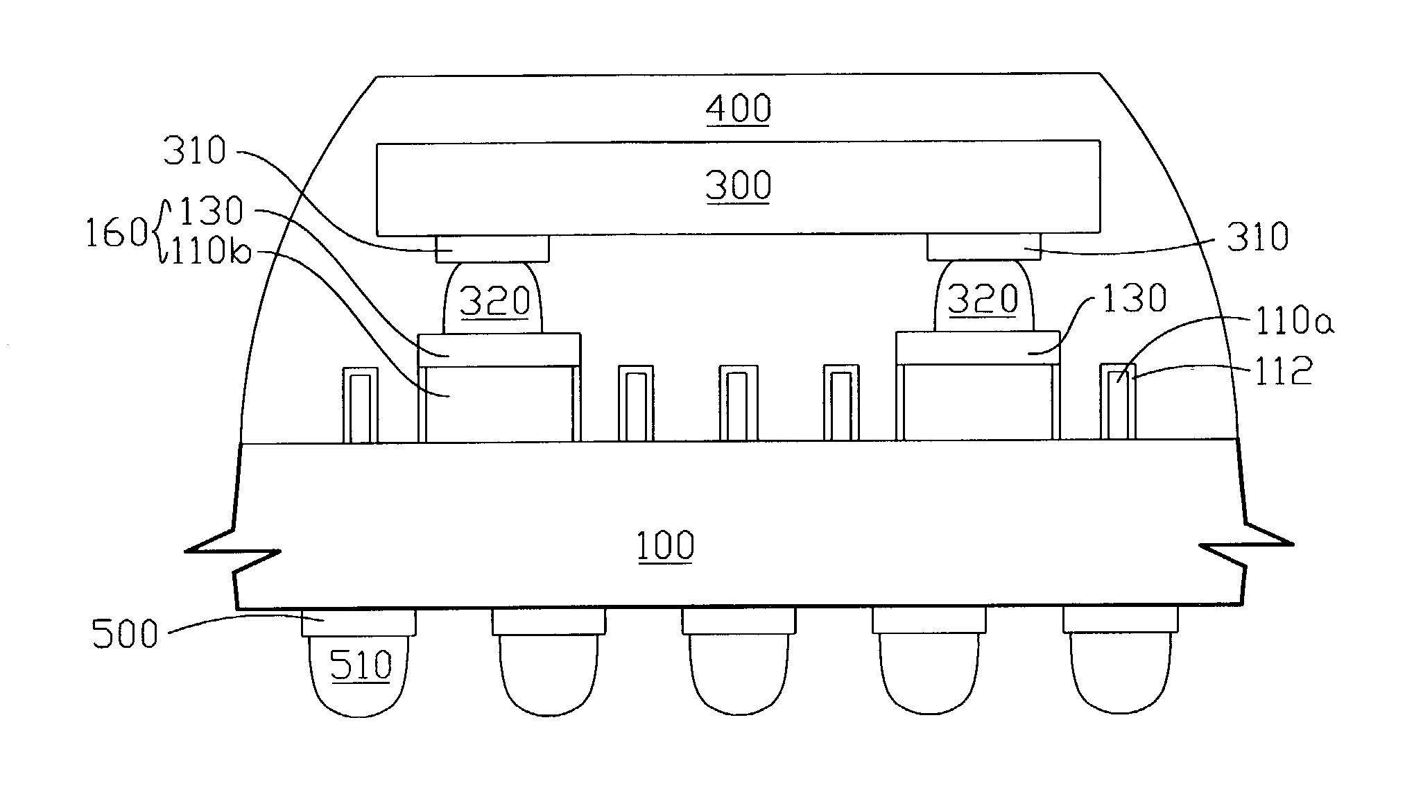
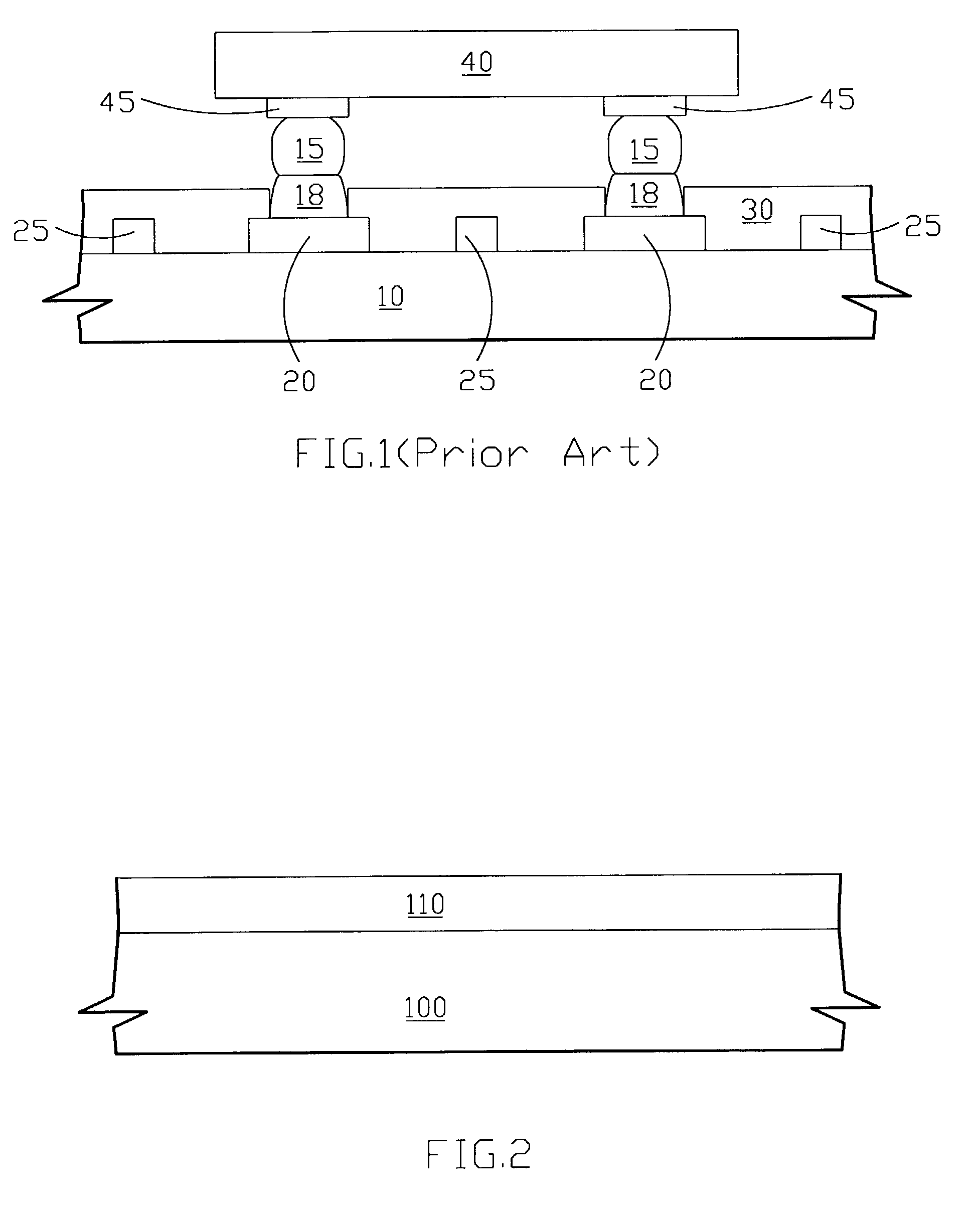
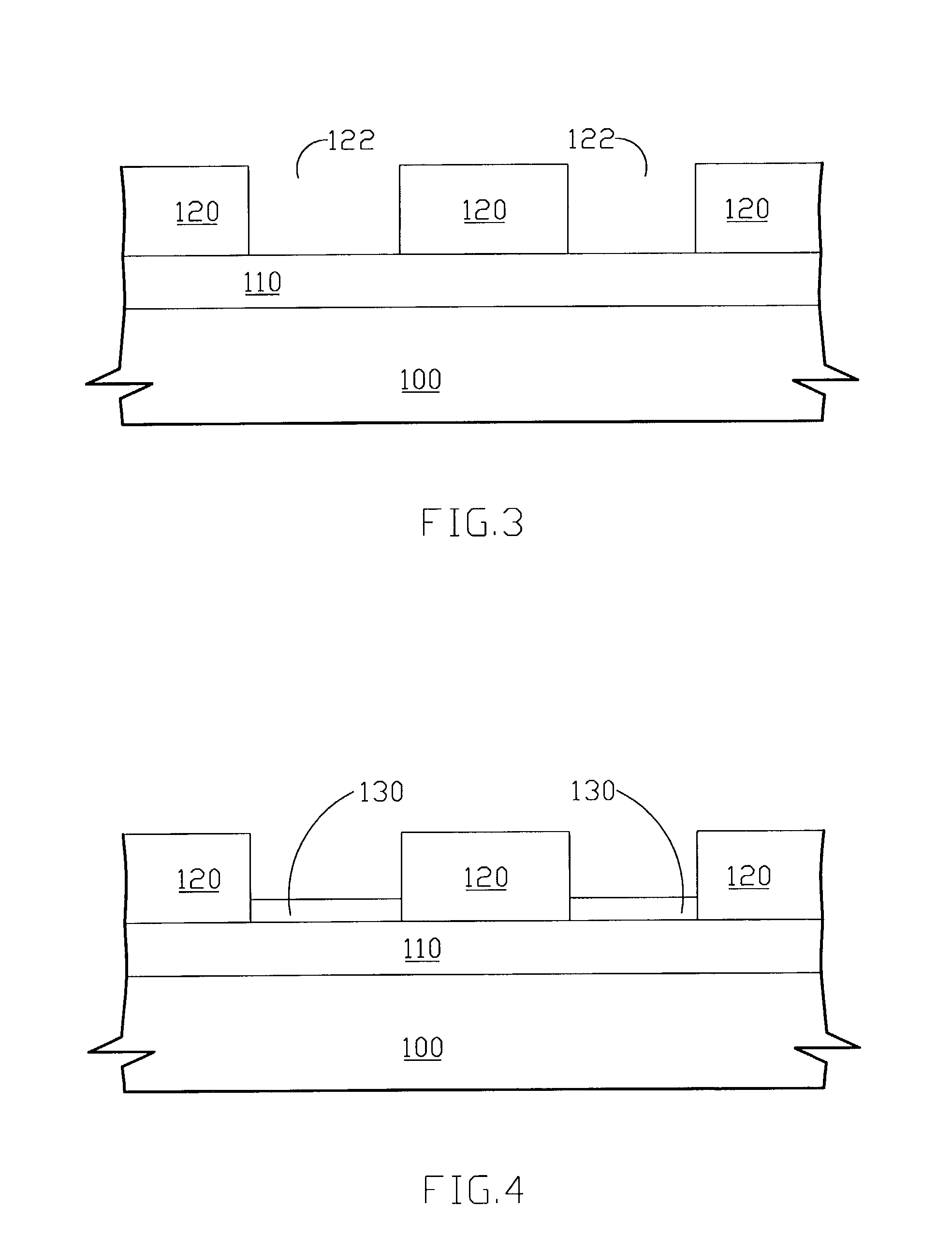
[0031]The present invention provides an integrated circuit package without a solder mask and a method for the same to avoid short circuit defects by using solder wettable metal as the material of the first solder pad and when forming an insulating layer whose material is solder non-wettable metal on the top surface and sidewall surface of the metal layer which is used as the circuit. Referring to FIG. 2, this shows a diagram in forming a metal layer on the substrate. The inner circuits of the substrate are omitted because those are not key points of the present invention. At first, a substrate 100 is provided and a metal layer 110 is formed on the substrate 100 of the present invention. A material of the metal l...


PUM

PropertyMeasurementUnit
Densityaaaaaaaaaa
Wettabilityaaaaaaaaaa
aaaaaaaaaa

Abstract

This invention relates to an integrated circuit package and a method for the same, especially relates to the integrated circuit package without a solder mask and the method for the same. A solder wettable metal is used as the material of the first solder pad and a non-wettable insulating layer is formed on the top surface and sidewalls of the metal layer, which is not solder pads, in the integrated circuit packages without a solder mask of the present invention to avoid short circuit defects and to increase a circuit density and reliability of the integrated circuit packages.

Description

BACKGROUND OF THE INVENTION[0001]1. Field of the Invention[0002]This invention relates to an integrated circuit package structure and a method for the same, especially relates to the integrated circuit package without a solder mask and the method for the same to increase a circuit density and the reliability of the integrated circuit package.[0003]2. Description of the Prior Art[0004]Integrated circuits are typically housed within a plastic package, for example a quad flat pack (QFP). Flat packs contain a lead frame, which has a plurality of leads that are connected to an integrated circuit die. The die is encapsulated by a hard plastic housing, which mechanically supports and electrically insulates the integrated circuit. The leads are typically soldered to a printed circuit board.[0005]Packaging techniques for integrated circuits have been developed in the past in an attempt to satisfy demands for miniaturization in the integrated circuit industry. Improved methods for miniaturiza...

Claims


Application Information

Patent Timeline
IPC IPC(8): H01L21/44B23K31/02H01L23/498H05K3/06H05K3/24H05K3/34
CPCH01L23/498H01L23/49816H01L24/16H05K3/3452H05K3/064H05K3/243H01L2224/16225H05K2201/2081H05K2203/0315H01L2924/15311H01L2224/05568H01L2224/05573H01L2924/00014H01L2924/14H01L2924/181H01L2924/00H01L2224/05599
Inventor HO, KUN-YAOKUNG, MORISS
Owner VIA TECH INC
Features
  • Generate Ideas
  • Intellectual Property
  • Life Sciences
  • Materials
  • Tech Scout
  • Unparalleled Data Quality
  • Higher Quality Content
  • 60% Fewer Hallucinations
Learn More