Boosting circuit

Inactive Publication Date: 2006-09-05
SAMSUNG ELECTRONICS CO LTD
View PDF12 Cites 7 Cited by
  • Summary
  • Abstract
  • Description
  • Claims
  • Application Information

AI Technical Summary

Benefits of technology

[0013]The present invention has been devised to solve the above problems, so it is an object of the present invention to provide a boosting circuit having a broader differentiable frequency bandwid

Problems solved by technology

Therefore, there is a drawback in that an additional tuning circuit is needed to prevent such influences.
Further, there exists a problem in that power consumption becomes high and frequency characteristics are deteriorated, since a two-stage process is needed to differentiate and then convert input voltages into currents.
However, unlike the boosting circuit of FIG. 1, an output of an output amplifier constructed with the NMOS transistors M1 and M4, current sources IB, and so on, is

Method used


Image

  • Boosting circuit
  • Boosting circuit
  • Boosting circuit

Examples


Embodiment Construction

[0025]Hereinafter, the present invention will be described in detail with reference to the accompanying drawings.

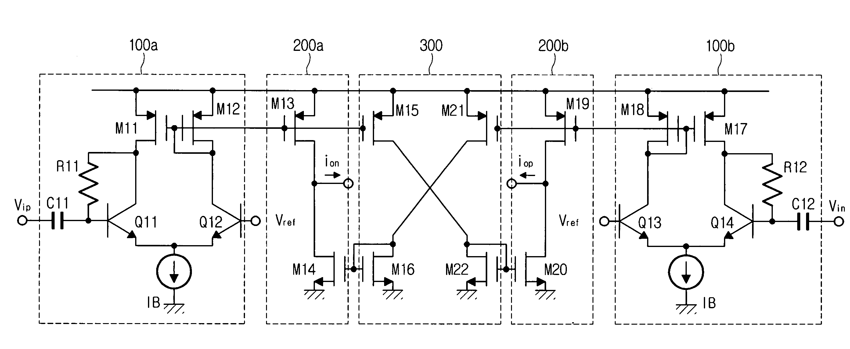
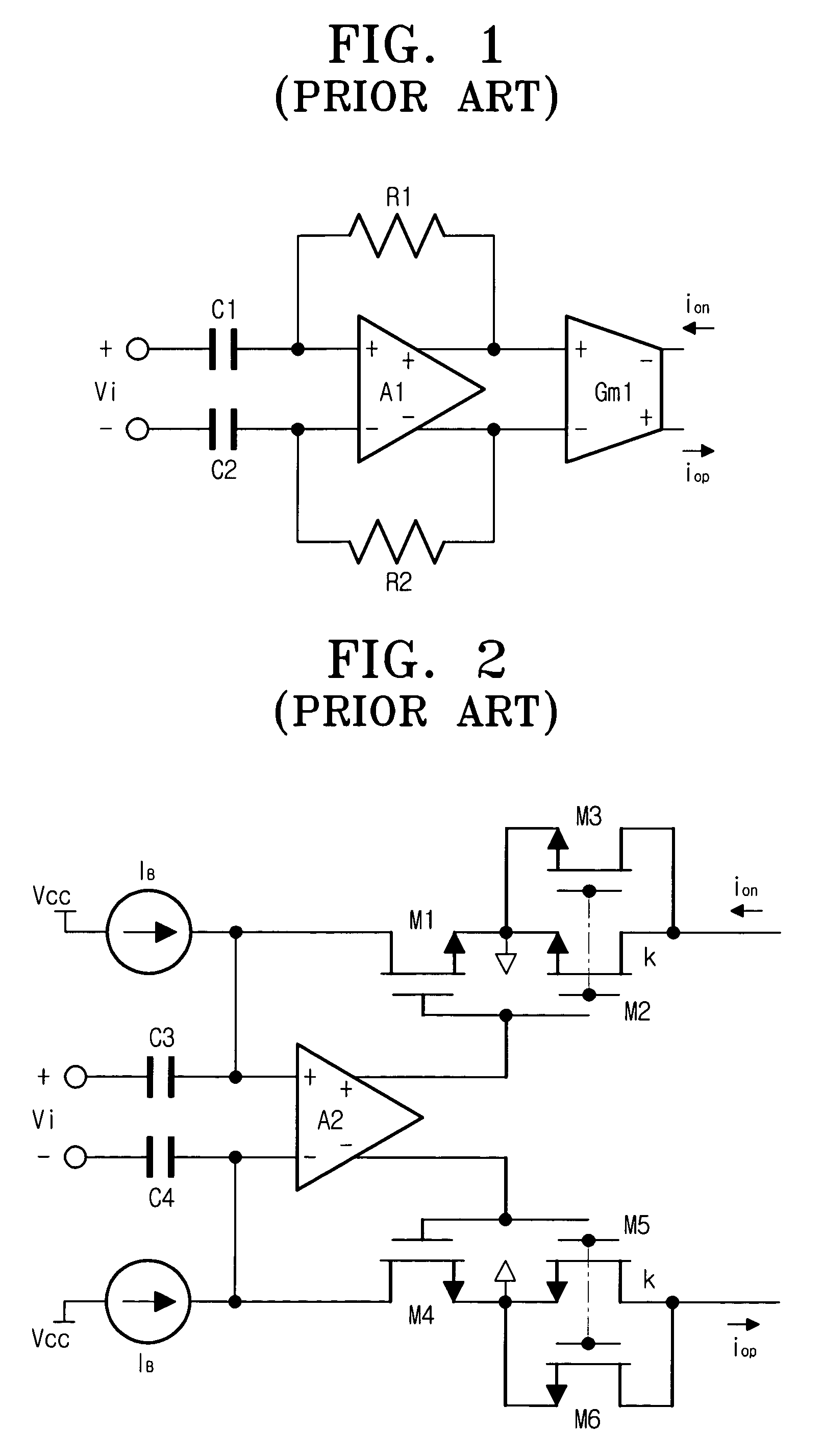
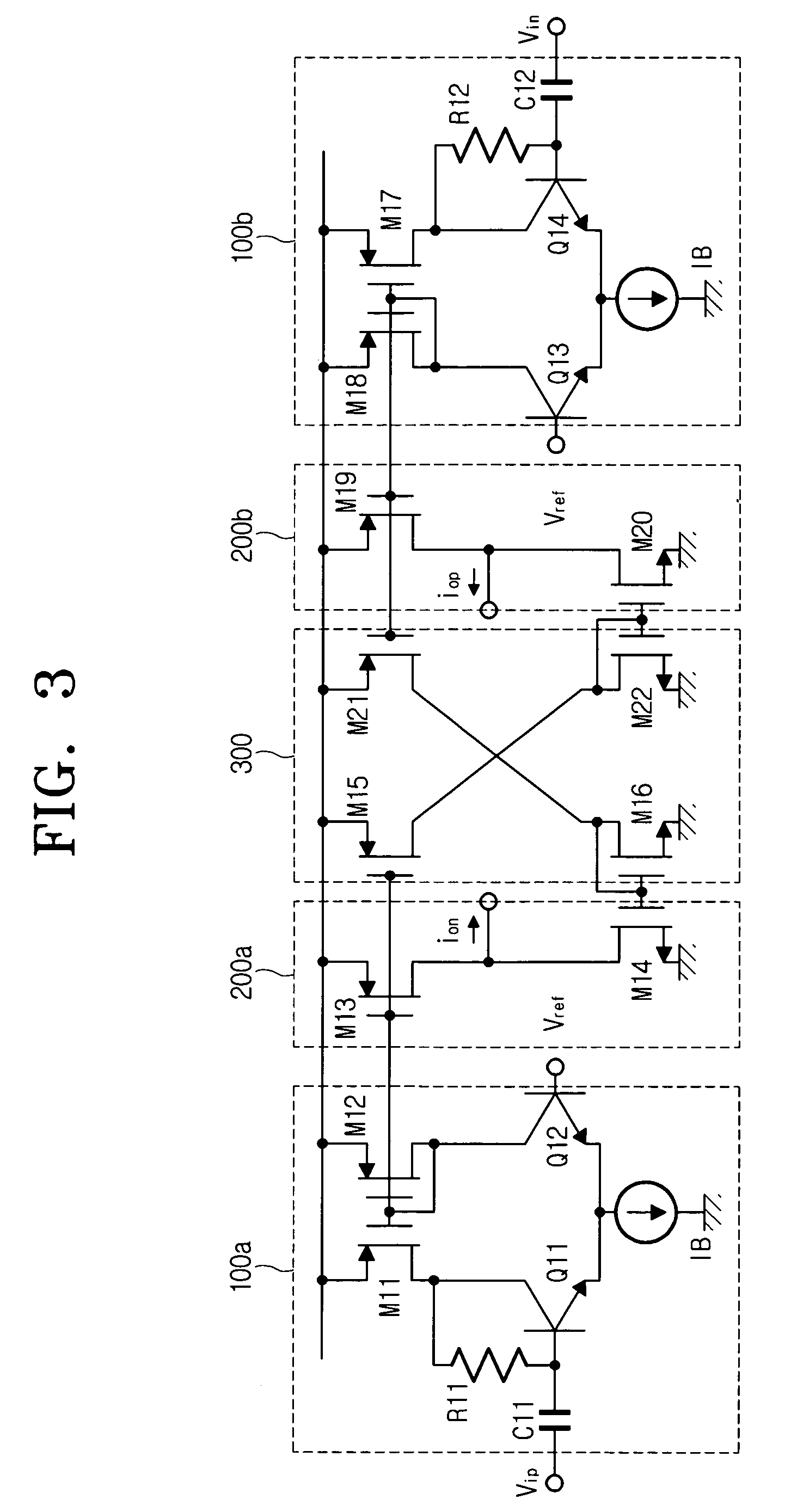
[0026]FIG. 3 is a view for showing a boosting circuit according to an embodiment of the present invention. The boosting circuit is structured with input circuit parts 100a and 100b, output circuit parts 200a and 200b, and a bias circuit part 300.

[0027]The input circuit parts 100a and 100b each outputs a differential current proportional to a differentiation of an input voltage. The bias circuit part 300 mirrors currents outputted from the input circuit parts 100a and 100b in order to reflect signals in the push-pull form, and produces inverted mirror currents. The output circuit parts 200a and 200b determine the magnitudes of the currents outputted from the input circuit parts 100a and 100b, and the bias circuit part 300 based on a size ratio of MOS transistors M13 and M15, that is, a ratio, k, of Width value(W) / Length value(L), add and output the magnitudes in the push-p...


PUM


Abstract

A boosting circuit is disclosed. The boosting circuit includes an input circuit part for outputting a differential current proportional to input voltages; a bias circuit part for mirroring the differential current, and producing an inverted differential current that the differential current is inverted; and an output circuit part for adjusting magnitudes of the differential current and the inverted differential current based on a predetermined ratio of MOS transistors, respectively, adding the adjusted differential current and inverted differential current, and producing an output current in a push-pull form. Accordingly, the boosting circuit has a broad maximum differentiable frequency bandwidth, and facilitates the adjustments of differentiation characteristics of an output current. Further, an amount of output current of differentiation form is not affected by external factors such as voltages, processes, temperatures, and so on.

Description

[0001]This application claims the priority of Korean Patent Application No. 2003-4626, filed on Jan. 23, 2003, in the Korean Intellectual Property Office, the disclosure of which is incorporated herein by reference in its entirety.BACKGROUND OF THE INVENTION[0002]1. Field of the Invention[0003]The present invention relates to a boosting circuit, and more particularly, to a boosting circuit to be used for a high frequency equalizer without having the amount of boost affected by external factors of not only frequency operation characteristics, but also voltages, processes, temperatures, and so on.[0004]2. Description of the Related Art[0005]The boosting circuit for an equalizer employed in optical recording / reproducing devices or hard disk drives for compact disk (CD) / digital video disk (DVD) is required to output differential currents from input voltages, and to adjust the amount of boost without affecting group delay characteristics up to a high frequency bandwidth of about 100 MHz....

Claims


Application Information

Patent Timeline
IPC IPC(8): H03F3/45H03F1/30G11B20/10H03F3/08H03F3/30H03K5/00H03K5/24
CPCH03K5/2481H03F3/3062H03F3/3023G11B20/10009H03K5/00
Inventor LEE, JEONG-WONMOON, JAE-JUNCHANG, SOO-JUNG
Owner SAMSUNG ELECTRONICS CO LTD
Why Eureka
Try Eureka